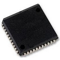
SC16C550BIA44 NXP Semiconductors, SC16C550BIA44 Datasheet - Page 6

SC16C550BIA44
Manufacturer Part Number
SC16C550BIA44
Description
UART, 16BYTE FIFO, 16C550, PLCC44
Manufacturer
NXP Semiconductors
Datasheet
1.SC16C550BIA44518.pdf
(48 pages)
Specifications of SC16C550BIA44
No. Of Channels
1
Data Rate
3Mbps
Supply Voltage Range
2.25V To 5.5V
Operating Temperature Range
-40°C To +85°C
Digital Ic Case Style
PLCC
No. Of Pins
44
Svhc
No SVHC (18-Jun-2010)
Operating
RoHS Compliant
Uart Features
Automatic Hardware Flow Control, Software Selectable Baud Rate Generator
Rohs Compliant
Yes
Available stocks
Company
Part Number
Manufacturer
Quantity
Price
Company:
Part Number:
SC16C550BIA44
Manufacturer:
NXPLIPS
Quantity:
3 000
Part Number:
SC16C550BIA44
Manufacturer:
NXP/恩智浦
Quantity:
20 000
Company:
Part Number:
SC16C550BIA44
Manufacturer:
NXP
Quantity:
15 318
Company:
Part Number:
SC16C550BIA44,512
Manufacturer:
NXP Semiconductors
Quantity:
10 000
Company:
Part Number:
SC16C550BIA44,518
Manufacturer:
NXP Semiconductors
Quantity:
10 000
NXP Semiconductors
Table 2.
SC16C550B_5
Product data sheet
Symbol
A0
A1
A2
AS
BAUDOUT
CS0
CS1
CS2
CS
CTS
D7 to D0
DCD
DDIS
[2]
[2]
[2]
[2]
[2]
[2]
Pin description
Pin
PLCC44 LQFP48 DIP40 HVQFN32
31
30
29
28
17
14
15
16
-
40
9, 8, 7,
6, 5, 4,
3, 2
42
26
5.2 Pin description
28
27
26
24
12
9
10
11
-
38
4, 3, 2,
47, 46,
45, 44,
43
40
22
28
27
26
25
15
12
13
14
-
36
8, 7,
6, 5,
4, 3,
2, 1
38
23
19
18
17
-
-
-
-
-
8
24
5, 4, 3, 1,
32, 31,
30, 29
26
-
Rev. 05 — 1 October 2008
Type
I
I
O
I
I
I/O
I
O
Description
Register select. A2 to A0 are used during read and write
operations to select the UART register to read from or
write to. Refer to
AS description.
Address strobe. When AS is active (LOW), A0, A1, and
A2 and CS0, CS1, and CS2 drive the internal select logic
directly; when AS is HIGH, the register select and chip
select signals are held at the logic levels they were in when
the LOW-to-HIGH transition of AS occurred.
Baud out. BAUDOUT is a 16 clock signal for the
transmitter section of the UART. The clock rate is
established by the reference oscillator frequency divided
by a divisor specified in the baud generator divisor latches.
BAUDOUT may also be used for the receiver section by
tying this output to RCLK. In HVQFN32 package
BAUDOUT and RCLK are bonded internally.
Chip select. When CS0 and CS1 are HIGH and CS2 is
LOW, these three inputs select the UART. When any of
these inputs are inactive, the UART remains inactive (refer
to AS description).
Clear to send. CTS is a modem status signal. Its condition
can be checked by reading bit 4 (CTS) of the Modem
Status Register. Bit 0 (CTS) of the Modem Status Register
indicates that CTS has changed states since the last read
from the Modem Status Register. If the modem status
interrupt is enabled when CTS changes levels and the
auto-CTS mode is not enabled, an interrupt is generated.
This pin has no effect on the UART’s transmit or receive
operation.
Data bus. Eight data lines with 3-state outputs provide a
bidirectional path for data, control and status information
between the UART and the CPU.
Data carrier detect. DCD is a modem status signal. Its
condition can be checked by reading bit 7 (DCD) of the
Modem Status Register. Bit 3 (DCD) of the Modem Status
Register indicates that DCD has changed states since the
last read from the Modem Status Register. If the modem
status interrupt is enabled when DCD changes levels, an
interrupt is generated.
Driver disable. DDIS is active (LOW) when the CPU is
reading data. When inactive (HIGH), DDIS can disable an
external transceiver.
5 V, 3.3 V and 2.5 V UART with 16-byte FIFOs
Table 3
for register addresses and refer to
SC16C550B
© NXP B.V. 2008. All rights reserved.
6 of 48


