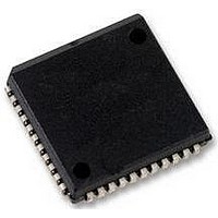
SC16C550BIA44 NXP Semiconductors, SC16C550BIA44 Datasheet - Page 9

SC16C550BIA44
Manufacturer Part Number
SC16C550BIA44
Description
UART, 16BYTE FIFO, 16C550, PLCC44
Manufacturer
NXP Semiconductors
Datasheet
1.SC16C550BIA44518.pdf
(48 pages)
Specifications of SC16C550BIA44
No. Of Channels
1
Data Rate
3Mbps
Supply Voltage Range
2.25V To 5.5V
Operating Temperature Range
-40°C To +85°C
Digital Ic Case Style
PLCC
No. Of Pins
44
Svhc
No SVHC (18-Jun-2010)
Operating
RoHS Compliant
Uart Features
Automatic Hardware Flow Control, Software Selectable Baud Rate Generator
Rohs Compliant
Yes
Available stocks
Company
Part Number
Manufacturer
Quantity
Price
Company:
Part Number:
SC16C550BIA44
Manufacturer:
NXPLIPS
Quantity:
3 000
Part Number:
SC16C550BIA44
Manufacturer:
NXP/恩智浦
Quantity:
20 000
Company:
Part Number:
SC16C550BIA44
Manufacturer:
NXP
Quantity:
15 318
Company:
Part Number:
SC16C550BIA44,512
Manufacturer:
NXP Semiconductors
Quantity:
10 000
Company:
Part Number:
SC16C550BIA44,518
Manufacturer:
NXP Semiconductors
Quantity:
10 000
NXP Semiconductors
Table 2.
[1]
[2]
[3]
6. Functional description
SC16C550B_5
Product data sheet
Symbol
IOW
IOW
XTAL1
XTAL2
HVQFN32 package die supply ground is connected to both the V
supply ground for proper device operation. For enhanced thermal, electrical, and board-level performance, the exposed pad needs to be
soldered to the board using a corresponding thermal pad on the board, and for proper heat conduction through the board thermal vias
need to be incorporated in the Printed-Circuit Board (PCB) in the thermal pad region.
This pin has a pull-up resistor.
In Sleep mode, XTAL2 is left floating.
[2]
[3]
Pin description
Pin
PLCC44 LQFP48 DIP40 HVQFN32
21
20
18
19
The SC16C550B provides serial asynchronous receive data synchronization,
parallel-to-serial and serial-to-parallel data conversions for both the transmitter and
receiver sections. These functions are necessary for converting the serial data stream into
parallel data that is required with digital data systems. Synchronization for the serial data
stream is accomplished by adding start and stop bits to the transmit data to form a data
character (character orientated protocol). Data integrity is insured by attaching a parity bit
to the data character. The parity bit is checked by the receiver for any transmission bit
errors. The SC16C550B is fabricated with an advanced CMOS process to achieve low
drain power and high speed requirements.
The SC16C550B is an upward solution that provides 16 bytes of transmit and receive
FIFO memory, instead of none in the 16C450. The SC16C550B is designed to work with
high speed modems and shared network environments that require fast data processing
time. Increased performance is realized in the SC16C550B by the larger transmit and
receive FIFOs. This allows the external processor to handle more networking tasks within
a given time. In addition, the four selectable levels of FIFO trigger interrupt are provided
for maximum data throughput performance, especially when operating in a multi-channel
environment. The combination of the above greatly reduces the bandwidth requirement of
the external controlling CPU, increases performance, and reduces power consumption.
The SC16C550B is capable of operation up to 3 Mbit/s with a 48 MHz external clock input
(at 5 V).
17
16
14
15
…continued
19
18
16
17
-
12
10
11
Rev. 05 — 1 October 2008
Type
I
I
O
SS
pin and the exposed center pad. The V
Description
Write inputs. When either IOW or IOW is active (LOW or
HIGH, respectively) and while the UART is selected, the
CPU is allowed to write control words or data into a
selected UART register. Only one of these inputs is
required to transfer data during a write operation; the other
input should be tied to its inactive level (that is, IOW tied
LOW or IOW tied HIGH).
Crystal connection or External clock input.
Crystal connection or the inversion of XTAL1 if XTAL1
is driven.
5 V, 3.3 V and 2.5 V UART with 16-byte FIFOs
SC16C550B
SS
pin must be connected to
© NXP B.V. 2008. All rights reserved.
9 of 48


