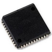
SCC68692C1A44 NXP Semiconductors, SCC68692C1A44 Datasheet - Page 23

SCC68692C1A44
Manufacturer Part Number
SCC68692C1A44
Description
UART, DUAL, SMD, 68692C1, PLCC44
Manufacturer
NXP Semiconductors
Datasheet
1.SCC68692C1A44518.pdf
(28 pages)
Specifications of SCC68692C1A44
No. Of Channels
2
Uart Features
Quadruple Buffered Receiver Data Register
Supply Voltage Range
4.5V To 5.5V
Operating Temperature Range
0°C To +70°C
Digital Ic Case Style
PLCC
No. Of Pins
44
Data Rate
115.2Kilobaud
Rohs Compliant
Yes
Lead Free Status / RoHS Status
Lead free / RoHS Compliant
Available stocks
Company
Part Number
Manufacturer
Quantity
Price
Company:
Part Number:
SCC68692C1A44
Manufacturer:
PHILIPS
Quantity:
991
Part Number:
SCC68692C1A44
Manufacturer:
PHILIPS/飞利浦
Quantity:
20 000
Company:
Part Number:
SCC68692C1A44,512
Manufacturer:
MICREL
Quantity:
143
Company:
Part Number:
SCC68692C1A44,512
Manufacturer:
NXP Semiconductors
Quantity:
10 000
Company:
Part Number:
SCC68692C1A44,518
Manufacturer:
NXP Semiconductors
Quantity:
10 000
Company:
Part Number:
SCC68692C1A44,529
Manufacturer:
NXP Semiconductors
Quantity:
10 000
OP2 through OP7. The data source for output ports OP0 and OP1 is
Philips Semiconductors
Output Port Notes
The output ports are controlled from four places: the OPCR register,
the OPR register, the MR registers and the command register. The
OPCR register controls the source of the data for the output ports
controlled by the MR and CR registers. When the OPR is the source
of the data for the output ports, the data at the ports is inverted from
that in the OPR register. The content of the OPR register is
controlled by the “Set Output Port Bits Command” and the “Reset
Output Bits Command”. These commands are at E and F,
respectively. When these commands are used, action takes place
only at the bit locations where ones exist. For example, a one in bit
location 5 of the data word used with the “Set Output Port Bits”
command will result in OPR5 being set to one. The OP5 would then
be set to zero (V
word associated with the “Reset Output Ports Bits” command would
set OPR5 to zero and, hence, the pin OP5 to a one (V
2004 Mar 03
OP0–OP7
Dual asynchronous receiver/transmitter (DUART)
TRANSMITTER
TxDA/B
D0–D7
INTRN
RECEIVER
ENABLED
ENABLED
(WRITE)
RxRDY
TxRDY
(SR2)
(SR0)
CSN
CSN
RxD
TxD
Figure 15. Test Conditions on Outputs
MR1(4:3) = 11
SS
MASTER STATION
PERIPHERAL STATION
MR1(4+3) = 11
). Similarly, a one in bit position 5 of the data
MR1(2) = 1
50pF
ADD#1 MR1(2) = 0 D0
150pF
BIT 9
0
ADD#1
2.7K
ADD#1 1
750
BIT 9
1
BIT 9
DD
).
ADD#1
Figure 14. Wake-Up Mode
D0
SD00151
D0
+5V
2.15V
BIT 9
0
BIT 9
0
23
STATUS DATA
pin, its meaning is not RTS at all. It is, rather, that the transmitter has
transmitter. Therefore, one could say that RTS and CTS are different
present character being serialized. It is usually the RTS output of the
with four valid characters in the receiver. When MR2(4) is set to one,
The CTS, RTS, CTS Enable Tx signals
CTS (Clear To Send) is usually meant to be a signal to the
transmitter meaning that it may transmit data to the receiver. The
CTS input is on pin MPI. The CTS signal is active LOW; thus, it is
called CTS.
RTS is usually meant to be a signal from the receiver indicating that
the receiver is ready to receive data. It is also active LOW and is,
thus, called RTSN. RTSN is on pin MP0. A receiver’s RTS output
will usually be connected to the CTS input of the associated
ends of the same wire!
MR2(4) is the bit that allows the transmitter to be controlled by the
CTS pin (MPI). When this bit is set to one AND the CTS input is
driven HIGH, the transmitter will stop sending data at the end of the
receiver that will be connected to the transmitter’s CTS input. The
receiver will set RTS HIGH when the receiver FIFO is full AND the
start bit of the fourth character is sensed. Transmission then stops
CTSN must be at zero for the transmitter to operate. If MR2(4) is set
to zero, the MP pin will have no effect on the operation of the
transmitter.
MR1(7) is the bit that allows the receiver to control MP0. When MP0
is controlled by the receiver, the meaning of that pin will be RTS.
However, a point of confusion arises in that MP0 may also be
controlled by the transmitter. When the transmitter is controlling this
finished sending its last data byte. Programming the MP0 pin to be
D0
MR1(2) = 1 ADD#2
ADD#2 1
ADD#2 1
BIT 9
BIT 9
SCC68692
STATUS DATA
ADD#2
Product data
BIT 9
0
SD00120


