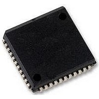
SCC68692C1A44 NXP Semiconductors, SCC68692C1A44 Datasheet - Page 7

SCC68692C1A44
Manufacturer Part Number
SCC68692C1A44
Description
UART, DUAL, SMD, 68692C1, PLCC44
Manufacturer
NXP Semiconductors
Datasheet
1.SCC68692C1A44518.pdf
(28 pages)
Specifications of SCC68692C1A44
No. Of Channels
2
Uart Features
Quadruple Buffered Receiver Data Register
Supply Voltage Range
4.5V To 5.5V
Operating Temperature Range
0°C To +70°C
Digital Ic Case Style
PLCC
No. Of Pins
44
Data Rate
115.2Kilobaud
Rohs Compliant
Yes
Lead Free Status / RoHS Status
Lead free / RoHS Compliant
Available stocks
Company
Part Number
Manufacturer
Quantity
Price
Company:
Part Number:
SCC68692C1A44
Manufacturer:
PHILIPS
Quantity:
991
Part Number:
SCC68692C1A44
Manufacturer:
PHILIPS/飞利浦
Quantity:
20 000
Company:
Part Number:
SCC68692C1A44,512
Manufacturer:
MICREL
Quantity:
143
Company:
Part Number:
SCC68692C1A44,512
Manufacturer:
NXP Semiconductors
Quantity:
10 000
Company:
Part Number:
SCC68692C1A44,518
Manufacturer:
NXP Semiconductors
Quantity:
10 000
Company:
Part Number:
SCC68692C1A44,529
Manufacturer:
NXP Semiconductors
Quantity:
10 000
1. Parameters are valid over specified temperature range.
2. All voltage measurements are referenced to ground (GND). For testing, all inputs swing between 0.4 V and 2.4 V with a transition time of
Philips Semiconductors
AC CHARACTERISTICS
NOTES:
2004 Mar 03
Reset Timing
Bus Timing5
Port Timing
Interrupt Timing
Clock Timing
Transmitter Timing
Receiver Timing
SYMBOL
SYMBOL
t
t
t
t
t
t
t
t
t
t
t
t
t
t
t
t
t
I
t
t
t
t
t
t
f
t
f
t
f
t
f
t
t
t
t
RES
AS
AH
RWS
RWH
CSW
CSD
DD
DA
DF
DI
DS
DH
DAL
DCR
DCW
DAH
DAT
CSC
PS
PH
PD
IR
CLK
CLK
CTC
CTC
RX
RX
TX
TX
TXD
TCS
RXS
RXH
Dual asynchronous receiver/transmitter (DUART)
5 ns maximum. For X1/CLK this swing is between 0.4 V and 4.4 V. All time measurements are referenced at input voltages of 0.8 V and
2.0 V and output voltages of 0.8 V and 2.0 V, as appropriate.
8
10
8
9
8
9
11
9
7
9
8
5
FIGURE
FIGURE
4,5,6
4,5,6
4,5,6
4,5,6
4,5,6
4,5,6
4,5,6
4,5,6
4,5,6
4,5,6
4,5,6
4,5,6
4,5,6
4,5,6
4,5,6
4,5,6
1
4
4
7
7
7
6
7
7
7
7
7
7
7
7
8
8
9
9
RESET pulse width
A1–A4 set-up time to CSN LOW
A1–A4 hold time from CSN LOW
RWN set-up time to CSN HIGH
RWN holdup time to CSN HIGH
CSN HIGH pulse width
CSN or IACKN HIGH from DTACKN LOW
Data valid from CSN or IACKN LOW
RDN LOW to data bus active
Data bus floating from CSN or IACKN HIGH
RDN HIGH to data bus invalid
Data set-up time to CLK HIGH
Data hold time from CSN HIGH
DTACKN LOW from read data valid
DTACKN LOW (read cycle) from CLK HIGH
DTACKN LOW (write cycle) form CLK HIGH
DTACKN HIGH from CSN or IACKN HIGH
DTACKN high-impedance from CSN or IACKN HIGH
CSN or IACKN set-up time to clock HIGH
Port input set-up time to CSN LOW
Port input hold time from CSN HIGH
Port output valid from CSN HIGH
INTRN (or OP3–OP7 when used as interrupts) negated from:
X1/CLK HIGH or LOW time
X1/CLK frequency
CTCLK (IP2) HIGH or LOW time
CTCLK (IP2) frequency
RxC HIGH or LOW time
RxC frequency (16X)
TxC HIGH or LOW time
TxC frequency (16X)
TxD output delay from TxC external clock input on IP pin
Output delay from TxC LOW at OP pin to TxD data output
RxD data set-up time before RxC HIGH at external clock input on IP pin
RxD data hold time after RxC HIGH at external clock input on IP pin
1, 2, 4
Read RHR (RxRDY/FFULL interrupt)
Write THR (TxRDY interrupt)
Reset command (break interrupt)
Stop C/T command (counter interrupt)
Read IPCR (input port change interrupt)
Write IMR (clear of interrupt mask bit)
(1X)
(1X)
PARAMETER
PARAMETER
7
Min
200
100
160
100
100
100
100
220
100
100
220
240
200
10
20
15
20
90
0
0
–
–
0
0
–
–
–
–
0
0
–
–
–
–
–
–
–
0
0
0
–
–
LIMITS
3.6864
Typ
–
–
–
–
–
–
–
–
–
–
–
–
–
–
–
–
–
–
–
–
–
–
–
–
–
–
–
–
–
–
–
–
–
–
–
–
–
–
–
–
–
3
SCC68692
Max
175
125
125
125
100
125
400
300
300
300
300
300
300
350
150
–
–
–
–
–
–
–
–
–
–
–
–
–
–
–
–
4
–
4
–
2
1
–
2
1
–
–
Product data
UNIT
UNIT
MHz
MHz
MHz
MHz
MHz
MHz
ns
ns
ns
ns
ns
ns
ns
ns
ns
ns
ns
ns
ns
ns
ns
ns
ns
ns
ns
ns
ns
ns
ns
ns
ns
ns
ns
ns
ns
ns
ns
ns
ns
ns
ns
ns


