ISPLSI1016E-125LJN LATTICE SEMICONDUCTOR, ISPLSI1016E-125LJN Datasheet
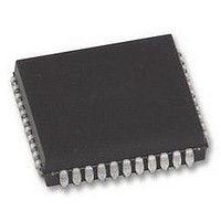
CMOS ISP EEPLD, SMD, 1016, PLCC44

ISPLSI1016E-125LJN

Manufacturer Part Number
ISPLSI1016E-125LJN
Description
CMOS ISP EEPLD, SMD, 1016, PLCC44
Manufacturer
LATTICE SEMICONDUCTOR
Datasheet

Specifications of ISPLSI1016E-125LJN

No. Of Macrocells
64
No. Of I/o's
32
Propagation Delay
7.5ns
Global Clock Setup Time
5.5ns
Frequency
125MHz
Supply Voltage Range
4.75V To 5.25V
Operating Temperature Range
0°C To +70°C
Logic
RoHS Compliant

Available stocks

Company
Part Number
Manufacturer
Quantity
Price
Company:
Part Number:
ISPLSI1016E-125LJN
Quantity:
103
Copyright © 2006 Lattice Semiconductor Corp. All brand or product names are trademarks or registered trademarks of their respective holders. The specifications and information herein are subject
to change without notice.
LATTICE SEMICONDUCTOR CORP., 5555 Northeast Moore Ct., Hillsboro, Oregon 97124, U.S.A.
Tel. (503) 268-8000; 1-800-LATTICE; FAX (503) 268-8556; http://www.latticesemi.com
1016e_09
• HIGH-DENSITY PROGRAMMABLE LOGIC
• HIGH-PERFORMANCE E
• IN-SYSTEM PROGRAMMABLE
• OFFERS THE EASE OF USE AND FAST SYSTEM
Features
— 2000 PLD Gates
— 32 I/O Pins, Four Dedicated Inputs
— 96 Registers
— High-Speed Global Interconnect
— Wide Input Gating for Fast Counters, State
— Small Logic Block Size for Random Logic
— TTL Compatible Inputs and Outputs
— Electrically Erasable and Reprogrammable
— Non-Volatile
— 100% Tested at Time of Manufacture
— Unused Product Term Shutdown Saves Power
— In-System Programmable (ISP™) 5V Only
— Increased Manufacturing Yields, Reduced Time-to-
— Reprogram Soldered Device for Faster Prototyping
— Complete Programmable Device Can Combine Glue
— Enhanced Pin Locking Capability
— Three Dedicated Clock Input Pins
— Synchronous and Asynchronous Clocks
— Programmable Output Slew Rate Control to
— Flexible Pin Placement
— Optimized Global Routing Pool Provides Global
— Lead-Free Package Options
SPEED OF PLDs WITH THE DENSITY AND FLEXIBILITY
OF FIELD PROGRAMMABLE GATE ARRAYS
Machines, Address Decoders, etc.
f
t
Market and Improved Product Quality
Logic and Structured Designs
Minimize Switching Noise
Interconnectivity
max = 125 MHz Maximum Operating Frequency
pd = 7.5 ns Propagation Delay
2
CMOS
®
TECHNOLOGY
1
In-System Programmable High Density PLD
The ispLSI 1016E is a High Density Programmable Logic
Device containing 96 Registers, 32 Universal I/O pins,
four Dedicated Input pins, three Dedicated Clock Input
pins, one Global OE input pin and a Global Routing Pool
(GRP). The GRP provides complete interconnectivity
between all of these elements. The ispLSI 1016E offers
5V non-volatile in-system programmability of the logic, as
well as the interconnect to provide truly reconfigurable
systems. A functional superset of the ispLSI 1016
architecture, the ispLSI 1016E device adds a new global
output enable pin.
The basic unit of logic on the ispLSI 1016E device is the
Generic Logic Block (GLB). The GLBs are labeled A0,
A1...B7 (see Figure 1). There are a total of 16 GLBs in the
ispLSI 1016E device. Each GLB has 18 inputs, a
programmable AND/OR/Exclusive OR array, and four
outputs which can be configured to be either combinatorial
or registered. Inputs to the GLB come from the GRP and
dedicated inputs. All of the GLB outputs are brought back
into the GRP so that they can be connected to the inputs
of any other GLB on the device.
Functional Block Diagram
Description
A0
A1
A2
A3
A4
A5
A6
A7
Global Routing Pool (GRP)
ispLSI
Logic
Array
D Q
D Q
D Q
D Q
GLB
®
1016E
B 6
B 5
B 4
B 3
B 2
B 1
B 0
B 7
CLK
August 2006
0139C1-isp

Related parts for ISPLSI1016E-125LJN

ISPLSI1016E-125LJN Summary of contents

Page 1

... Interconnectivity — Lead-Free Package Options Copyright © 2006 Lattice Semiconductor Corp. All brand or product names are trademarks or registered trademarks of their respective holders. The specifications and information herein are subject to change without notice. LATTICE SEMICONDUCTOR CORP., 5555 Northeast Moore Ct., Hillsboro, Oregon 97124, U.S.A. ...

Page 2

Functional Block Diagram Figure 1. ispLSI 1016E Functional Block Diagram Generic Logic Blocks (GLBs) I I/O 1 I I I I/O 9 I/O ...

Page 3

Absolute Maximum Ratings Supply Voltage V ................................. -0.5 to +7.0V CC Input Voltage Applied ........................ -2 Off-State Output Voltage Applied ..... -2 Storage Temperature ................................ -65 to 150°C Case Temp. with Power Applied .............. -55 to ...

Page 4

... Typical values are and T = 25° Maximum I varies widely with specific device configuration and operating frequency. Refer to the Power Consumption CC section of this data sheet and Thermal Management section of the Lattice Semiconductor Data Book or CD-ROM to estimate maximum Specifications ispLSI 1016E Figure 2. Test Load GND to 3 ...

Page 5

External Timing Parameters 4 TEST 2 PARAMETER # COND Data Prop. Delay, 4PT Bypass, ORP Bypass pd1 Data Prop. Delay, Worst Case Path pd2 Clk. Frequency with Int. Feedback max f ...

Page 6

Internal Timing Parameters 2 PARAMETER # Inputs t 22 I/O Register Bypass iobp t 23 I/O Latch Delay iolat t 24 I/O Register Setup Time before Clock iosu t 25 I/O Register Hold Time after Clock ioh t 26 I/O ...

Page 7

Internal Timing Parameters 2 PARAMETER # Outputs t 49 Output Buffer Delay Output Slew Limited Delay Adder I/O Cell OE to Output Enabled oen t 52 I/O Cell OE to Output Disabled odis t ...

Page 8

Timing Model I/O Cell Ded. In #28 I/O Reg Bypass I/O Pin #22 (Input) Input Loading Register Q D RST #29, 31, 32 #59 # Reset Distribution Y1,2 Y0 GOE Derivations of ...

Page 9

Maximum GRP Delay vs GLB Loads Power Consumption Power consumption in the ispLSI 1016E device depends on two primary factors: the speed at which the device is operating and the number of Product Terms used. Figure 3. Typical Device Power ...

Page 10

Pin Description PLCC NAME PIN NUMBERS I I/O 3 15, 16, 17, 18, 13, I I/O 7 19, 20, 21, 22, I I/O 11 25, 26, 27, 28, 19, 23, I I/O ...

Page 11

Pin Configurations ispLSI 1016E 44-Pin PLCC Pinout Diagram I/O 28 I/O 29 I/O 30 I/O 31 ispEN 1 SDI/ Pins have dual function capability. 2. Pins have dual function capability which is software selectable. ispLSI 1016E 44-Pin TQFP ...

Page 12

Part Number Description ispLSI Device Family Device Number Speed 125 = 125 MHz fmax 100 = 100 MHz fmax MHz fmax ispLSI 1016E Ordering Information Conventional Packaging FAMILY fmax (MHz) tpd (ns) 125 125 100 ispLSI 100 ...

Page 13

Revision History Date Version — 08 August 2006 09 Specifications ispLSI 1016E Change Summary Previous Lattice release. Updated for lead-free package options. 13 ...

Related keywords