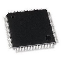
LC4256V-75TN100C LATTICE SEMICONDUCTOR, LC4256V-75TN100C Datasheet - Page 24

LC4256V-75TN100C
Manufacturer Part Number
LC4256V-75TN100C
Description
MACH4000 ISP CPLD, 4256, TQFP100
Manufacturer
LATTICE SEMICONDUCTOR
Series
IspMACH 4000r
Datasheet
1.LC4064V-75TN44C.pdf
(94 pages)
Specifications of LC4256V-75TN100C
No. Of Macrocells
256
No. Of I/o's
64
Propagation Delay
7.5ns
Global Clock Setup Time
4.5ns
Frequency
322MHz
Supply Voltage Range
3V To 3.6V
Operating Temperature Range
0°C
Lead Free Status / RoHS Status
Lead free / RoHS Compliant
Available stocks
Company
Part Number
Manufacturer
Quantity
Price
Company:
Part Number:
LC4256V-75TN100C
Manufacturer:
LATTICE
Quantity:
2 940
Company:
Part Number:
LC4256V-75TN100C
Manufacturer:
LATTICE32
Quantity:
750
Company:
Part Number:
LC4256V-75TN100C
Manufacturer:
Lattice Semiconductor Corporation
Quantity:
10 000
Part Number:
LC4256V-75TN100C
Manufacturer:
LATTICE
Quantity:
20 000
Lattice Semiconductor
ispMACH 4000Z External Switching Characteristics
t
t
t
t
t
t
t
t
t
t
t
t
t
t
t
t
t
t
t
f
t
1. Timing numbers are based on default LVCMOS 1.8 I/O buffers. Use timing adjusters provided to calculate other standards.
2. Measured using standard switching GRP loading of 1 and 1 output switching.
3. Pulse widths and clock widths less than minimum will cause unknown behavior.
4. Standard 16-bit counter using GRP feedback.
PD
PD_MC
S
ST
SIR
SIRZ
H
HT
HIR
HIRZ
CO
R
RW
PTOE/DIS
GPTOE/DIS
GOE/DIS
CW
GW
WIR
MAX
MAX
Parameter
4
(Ext.)
5-PT bypass combinatorial propagation delay
20-PT combinatorial propagation delay
through macrocell
GLB register setup time before clock
GLB register setup time before clock with
T-type register
GLB register setup time before clock, input
register path
GLB register setup time before clock with zeto
hold
GLB register hold time after clock
GLB register hold time after clock with T-type
register
GLB register hold time after clock, input
register path
GLB register hold time after clock, input
register path with zero hold
GLB register clock-to-output delay
External reset pin to output delay
External reset pulse duration
Input to output local product term output
enable/disable
Input to output global product term output
enable/disable
Global OE input to output enable/disable
Global clock width, high or low
Global gate width low (for low transparent) or
high (for high transparent)
Input register clock width, high or low
Clock frequency with internal feedback
clock frequency with external feedback,
[1 / (t
S
+ t
CO
)]
Description
Over Recommended Operating Conditions
1, 2, 3
24
Min.
267
192
2.2
2.4
1.0
2.0
0.0
0.0
1.0
0.0
1.5
1.0
1.0
1.0
—
—
—
—
—
—
—
ispMACH 4000V/B/C/Z Family Data Sheet
-35
Max.
3.5
4.4
3.0
5.0
7.0
6.5
4.5
—
—
—
—
—
—
—
—
—
—
—
—
—
—
Min.
250
175
2.5
2.7
1.1
2.1
0.0
0.0
1.0
0.0
1.7
1.5
1.5
1.5
—
—
—
—
—
—
—
-37
Max.
3.7
4.7
3.2
6.0
8.0
7.0
4.5
—
—
—
—
—
—
—
—
—
—
—
—
—
—
Min.
161
220
2.7
2.9
1.3
2.6
0.0
0.0
1.3
0.0
2.0
1.8
1.8
1.8
—
—
—
—
—
—
—
-42
Max.
4.2
5.7
3.5
7.3
8.0
8.0
4.8
—
—
—
—
—
—
—
—
—
—
—
—
—
—
Timing v.2.2
Units
MHz
MHz
ns
ns
ns
ns
ns
ns
ns
ns
ns
ns
ns
ns
ns
ns
ns
ns
ns
ns
ns


