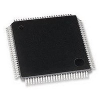
LC4256V-75TN100C LATTICE SEMICONDUCTOR, LC4256V-75TN100C Datasheet - Page 3

LC4256V-75TN100C
Manufacturer Part Number
LC4256V-75TN100C
Description
MACH4000 ISP CPLD, 4256, TQFP100
Manufacturer
LATTICE SEMICONDUCTOR
Series
IspMACH 4000r
Datasheet
1.LC4064V-75TN44C.pdf
(94 pages)
Specifications of LC4256V-75TN100C
No. Of Macrocells
256
No. Of I/o's
64
Propagation Delay
7.5ns
Global Clock Setup Time
4.5ns
Frequency
322MHz
Supply Voltage Range
3V To 3.6V
Operating Temperature Range
0°C
Lead Free Status / RoHS Status
Lead free / RoHS Compliant
Available stocks
Company
Part Number
Manufacturer
Quantity
Price
Company:
Part Number:
LC4256V-75TN100C
Manufacturer:
LATTICE
Quantity:
2 940
Company:
Part Number:
LC4256V-75TN100C
Manufacturer:
LATTICE32
Quantity:
750
Company:
Part Number:
LC4256V-75TN100C
Manufacturer:
Lattice Semiconductor Corporation
Quantity:
10 000
Part Number:
LC4256V-75TN100C
Manufacturer:
LATTICE
Quantity:
20 000
Lattice Semiconductor
Figure 1. Functional Block Diagram
The I/Os in the ispMACH 4000 are split into two banks. Each bank has a separate I/O power supply. Inputs can
support a variety of standards independent of the chip or bank power supply. Outputs support the standards com-
patible with the power supply provided to the bank. Support for a variety of standards helps designers implement
designs in mixed voltage environments. In addition, 5V tolerant inputs are specified within an I/O bank that is con-
nected to V
ispMACH 4000 Architecture
There are a total of two GLBs in the ispMACH 4032, increasing to 32 GLBs in the ispMACH 4512. Each GLB has
36 inputs. All GLB inputs come from the GRP and all outputs from the GLB are brought back into the GRP to be
connected to the inputs of any other GLB on the device. Even if feedback signals return to the same GLB, they still
must go through the GRP. This mechanism ensures that GLBs communicate with each other with consistent and
predictable delays. The outputs from the GLB are also sent to the ORP. The ORP then sends them to the associ-
ated I/O cells in the I/O block.
Generic Logic Block
The ispMACH 4000 GLB consists of a programmable AND array, logic allocator, 16 macrocells and a GLB clock
generator. Macrocells are decoupled from the product terms through the logic allocator and the I/O pins are decou-
pled from macrocells through the ORP. Figure 2 illustrates the GLB.
CCO
Block
Block
I/O
I/O
of 3.0V to 3.6V for LVCMOS 3.3, LVTTL and PCI interfaces.
ORP
ORP
16
16
Generic
Generic
Block
Block
Logic
Logic
16
16
36
36
3
ispMACH 4000V/B/C/Z Family Data Sheet
36
36
16
16
Generic
Generic
Block
Block
Logic
Logic
16
16
ORP
ORP
Block
Block
I/O
I/O


