ISPLSI2064A-100LJN84 LATTICE SEMICONDUCTOR, ISPLSI2064A-100LJN84 Datasheet
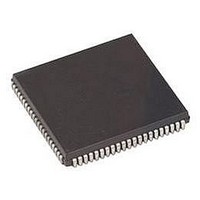
IC, PLD, EEPROM 64 MACROCELL 10NS LCC-84

ISPLSI2064A-100LJN84

Manufacturer Part Number
ISPLSI2064A-100LJN84
Description
IC, PLD, EEPROM 64 MACROCELL 10NS LCC-84
Manufacturer
LATTICE SEMICONDUCTOR
Series
IspLSI 2064Ar
Datasheet

Specifications of ISPLSI2064A-100LJN84

Cpld Type
EEPROM
No. Of Macrocells
64
No. Of I/o's
64
Propagation Delay
10ns
Global Clock Setup Time
6.5ns
Frequency
100MHz
Supply Voltage Range
4.75V To 5.25V
Lead Free Status / RoHS Status
Lead free / RoHS Compliant

Available stocks

Company
Part Number
Manufacturer
Quantity
Price
Part Number:
ISPLSI2064A-100LJN84
Manufacturer:
LATTICE
Quantity:
390
• ENHANCEMENTS
• HIGH DENSITY PROGRAMMABLE LOGIC
• HIGH PERFORMANCE E
• IN-SYSTEM PROGRAMMABLE
• OFFERS THE EASE OF USE AND FAST SYSTEM
Copyright © 2006 Lattice Semiconductor Corp. All brand or product names are trademarks or registered trademarks of their respective holders. The specifications and information herein are subject
to change without notice.
LATTICE SEMICONDUCTOR CORP., 5555 Northeast Moore Ct., Hillsboro, Oregon 97124, U.S.A.
Tel. (503) 268-8000; 1-800-LATTICE; FAX (503) 268-8556; http://www.latticesemi.com
2064_10
Features
— ispLSI 2064A is Fully Form and Function Compatible
— ispLSI 2064A is Built on an Advanced 0.35 Micron
— 2000 PLD Gates
— 64 I/O Pins, Four Dedicated Inputs
— 64 Registers
— High Speed Global Interconnect
— Wide Input Gating for Fast Counters, State
— Small Logic Block Size for Random Logic
— TTL Compatible Inputs and Outputs
— Electrically Erasable and Reprogrammable
— Non-Volatile
— 100% Tested at Time of Manufacture
— Unused Product Term Shutdown Saves Power
— In-System Programmable (ISP™) 5V Only
— Increased Manufacturing Yields, Reduced Time-to-
— Reprogram Soldered Devices for Faster Prototyping
SPEED OF PLDs WITH THE DENSITY AND FLEXIBILITY
OF FIELD PROGRAMMABLE GATE ARRAYS
— Complete Programmable Device Can Combine Glue
— Enhanced Pin Locking Capability
— Three Dedicated Clock Input Pins
— Synchronous and Asynchronous Clocks
— Programmable Output Slew Rate Control to
— Flexible Pin Placement
— Optimized Global Routing Pool Provides Global
— Lead-Free Package Options
f
t
Market and Improved Product Quality
Logic and Structured Designs
Machines, Address Decoders, etc.
Minimize Switching Noise
Interconnectivity
to the ispLSI 2064, with Identical Timing
Specifcations and Packaging
E
max = 125 MHz Maximum Operating Frequency
pd = 7.5 ns Propagation Delay
2
CMOS
®
Technology
2
CMOS
®
TECHNOLOGY
1
In-System Programmable High Density PLD
Fu
The ispLSI 2064 and 2064A are High Density Program-
mable Logic Devices. The devices contain 64 Registers,
64 Universal I/O pins, four Dedicated Input pins, three
Dedicated Clock Input pins, two dedicated Global OE
input pins and a Global Routing Pool (GRP). The GRP
provides complete interconnectivity between all of these
elements. The 2064 and 2064A feature 5V in-system
programmability and in-system diagnostic capabilities.
The ispLSI 2064 and 2064A offer non-volatile
reprogrammability of the logic, as well as the intercon-
nect, to provide truly reconfigurable systems.
The basic unit of logic on these devices is the Generic
Logic Block (GLB). The GLBs are labeled A0, A1…B7
(Figure 1). There are a total of 16 GLBs in the ispLSI 2064
and 2064A devices. Each GLB is made up of four
macrocells. Each GLB has 18 inputs, a programmable
AND/OR/Exclusive OR array, and four outputs which can
be configured to be either combinatorial or registered.
Inputs to the GLB come from the GRP and dedicated
inputs. All of the GLB outputs are brought back into the
GRP so that they can be connected to the inputs of any
GLB on the device.
Functional Block Diagram
Description
A0
A1
A2
A3
GLB
A4
Output Routing Pool (ORP)
ispLSI
B7
A5
Global Routing Pool
Output Routing Pool (ORP)
Logic
Array
Input Bus
(GRP)
D Q
D Q
D Q
D Q
B6
Input Bus
A6
B5
A7
®
2064/A
B4
August 2006
B0
B3
B2
B1
0139Bisp/2064

Related parts for ISPLSI2064A-100LJN84

ISPLSI2064A-100LJN84 Summary of contents

Page 1

... Interconnectivity — Lead-Free Package Options Copyright © 2006 Lattice Semiconductor Corp. All brand or product names are trademarks or registered trademarks of their respective holders. The specifications and information herein are subject to change without notice. LATTICE SEMICONDUCTOR CORP., 5555 Northeast Moore Ct., Hillsboro, Oregon 97124, U.S.A. ...

Page 2

Functional Block Diagram Figure 1. ispLSI 2064/A Functional Block Diagram Megablock I/O 0 I/O 1 I/O 2 I/O 3 I/O 4 I/O 5 I/O 6 I/O 7 I/O 8 I/O 9 I/O 10 I/O 11 I/O 12 I/O 13 I/O ...

Page 3

Absolute Maximum Ratings Supply Voltage V cc ................................................... Input Voltage Applied .............................. -2 Off-State Output Voltage Applied ........... -2 Storage Temperature ..................................... -65 to 150°C Case Temp. with Power Applied .................... -55 to 125°C Max. Junction ...

Page 4

... Typical values are and T = 25° Maximum I varies widely with specific device configuration and operating frequency. Refer to the Power Consumption CC section of this data sheet and Thermal Management section of the Lattice Semiconductor Data Book or CD-ROM to estimate maximum Specifications ispLSI 2064/A Figure 2. Test Load GND to 3 ...

Page 5

External Timing Parameters 4 TEST 2 PARAMETER # COND Data Propagation Delay, 4PT Bypass, ORP Bypass pd1 Data Propagation Delay pd2 Clock Frequency with Internal Feedback max f – 4 Clock ...

Page 6

Internal Timing Parameters 2 PARAMETER DESCRIPTION # Inputs Input Buffer Delay t din 21 Dedicated Input Delay GRP t grp 22 GRP Delay GLB t 4ptbp 4 Product Term Bypass Comb. Path Delay 23 t 4ptbp 24 ...

Page 7

Timing Model I/O Cell Ded. In #21 I/O Delay I/O Pin #20 (Input) #45 Reset Y0,1,2 GOE 0 Derivations of su, h and co from the Product Term Clock Logic + Reg ...

Page 8

Power Consumption Power consumption in the ispLSI 2064 and 2064A de- vices depends on two primary factors: the speed at which the device is operating and the number of Product Terms Figure 4. Typical Device Power Consumption vs fmax 160 ...

Page 9

Pin Description NAME PLCC PIN NUMBERS I I/O 3 26, 27, 30, 31, I I I/O 11 34, 35, 38, 39, I I I/O 19 45, ...

Page 10

Pin Description NAME TQFP PIN NUMBERS I I/O 3 17, 18, I I/O 7 21, 22, I I/O 11 29, 30, I I/O 15 33, 34, I I/O 19 40, ...

Page 11

Pin Configuration ispLSI 2064/A 84-Pin PLCC Pinout Diagram I I I/O 60 ...

Page 12

Pin Configuration ispLSI 2064/A 100-Pin TQFP Pinout Diagram ...

Page 13

Part Number Description ispLSI XXXXX Device Family 2064 2064A Device Number Speed f 125 = 125 MHz max f 100 = 100 MHz max MHz max ispLSI 2064/A Ordering Information Conventional Packaging FAMILY fmax (MHz) tpd ...

Page 14

Ordering Information (Cont.) Lead-Free Packaging FAMILY fmax (MHz) tpd (ns) 125 125 100 ispLSI 100 84-PLCC lead-free package is MSL4. Refer to “Handling Moisture Sensitive Packages” document on www.latticesemi.com. FAMILY fmax (MHz) tpd (ns) 81 ...

Related keywords