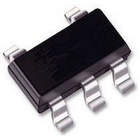
74LVC1G125GW NXP Semiconductors, 74LVC1G125GW Datasheet - Page 7

74LVC1G125GW
Manufacturer Part Number
74LVC1G125GW
Description
IC, LOGIC, 74LVC1G, BUFFER, UMT5
Manufacturer
NXP Semiconductors
Datasheet
1.74LVC1G125GW.pdf
(19 pages)
Specifications of 74LVC1G125GW
Supply Voltage Range
1.65V To 5.5V
Logic Case Style
SOT-353
No. Of Pins
5
Operating Temperature Range
-40°C To +125°C
Svhc
No SVHC (18-Jun-2010)
Logic Ic Base
RoHS Compliant
Package / Case
SOT-353
Logic Device Type
Buffer / Line Driver, Non Inverting
Rohs Compliant
Yes
Available stocks
Company
Part Number
Manufacturer
Quantity
Price
Company:
Part Number:
74LVC1G125GW
Manufacturer:
NXP
Quantity:
81 400
Company:
Part Number:
74LVC1G125GW
Manufacturer:
MACROBL
Quantity:
59
Part Number:
74LVC1G125GW
Manufacturer:
NXP/恩智浦
Quantity:
20 000
Company:
Part Number:
74LVC1G125GW(JB)
Manufacturer:
PHILIPS
Quantity:
140
Company:
Part Number:
74LVC1G125GW,125
Manufacturer:
NXP Semiconductors
Quantity:
4 300
Company:
Part Number:
74LVC1G125GWЈ¬125
Manufacturer:
NXP
Quantity:
15 000
NXP Semiconductors
11. Dynamic characteristics
Table 8.
Voltages are referenced to GND (ground = 0 V). For test circuit see
[1]
[2]
[3]
[4]
[5]
74LVC1G125
Product data sheet
Symbol Parameter
t
t
t
C
pd
en
dis
PD
Typical values are measured at T
t
t
t
C
P
f
f
C
V
N = number of inputs switching;
(C
pd
en
dis
i
o
D
CC
PD
= input frequency in MHz;
L
= output frequency in MHz;
is the same as t
is the same as t
= output load capacitance in pF;
= C
is the same as t
L
is used to determine the dynamic power dissipation (P
= supply voltage in V;
V
propagation delay A to Y; see
enable time
disable time
power dissipation
capacitance
PD
Dynamic characteristics
CC
V
2
f
CC
o
2
) = sum of outputs.
f
PLH
PZH
PLZ
i
N + (C
and t
and t
and t
PHL
PZL
PHZ
Conditions
OE to Y; see
OE to Y; see
per buffer; V
L
V
V
V
V
V
V
V
V
V
V
V
V
V
V
V
output enabled
output disabled
V
amb
CC
CC
CC
CC
CC
CC
CC
CC
CC
CC
CC
CC
CC
CC
CC
CC
= 1.65 V to 1.95 V
= 2.3 V to 2.7 V
= 2.7 V
= 3.0 V to 3.6 V
= 4.5 V to 5.5 V
= 1.65 V to 1.95 V
= 2.3 V to 2.7 V
= 2.7 V
= 3.0 V to 3.6 V
= 4.5 V to 5.5 V
= 1.65 V to 1.95 V
= 2.3 V to 2.7 V
= 2.7 V
= 3.0 V to 3.6 V
= 4.5 V to 5.5 V
= 25 C and V
2
f
Figure 7
o
All information provided in this document is subject to legal disclaimers.
I
) where:
Figure 8
Figure 8
= GND to V
Rev. 9 — 29 December 2010
CC
= 1.8 V, 2.5 V, 2.7 V, 3.3 V and 5.0 V respectively.
CC
D
in W).
[2]
[3]
[4]
[5]
Figure
Min
1.0
0.5
0.5
0.5
0.5
1.0
0.5
0.5
0.5
0.5
1.0
0.5
0.5
0.5
0.5
-
-
40 C to +85 C
9.
Typ
3.3
2.2
2.5
2.1
1.7
4.1
2.8
3.3
2.4
2.1
4.3
2.7
3.0
3.1
2.2
25
6
[1]
Max
8.0
5.5
5.5
4.5
4.0
9.4
6.6
6.6
5.3
5.0
9.2
5.0
5.0
5.0
4.2
-
-
Bus buffer/line driver; 3-state
74LVC1G125
40 C to +125 C Unit
Min
1.0
1.0
1.0
0.5
0.5
0.5
0.5
0.5
0.5
0.5
0.5
0.5
0.5
0.5
0.5
-
-
© NXP B.V. 2010. All rights reserved.
Max
10.5
5.5
8.5
8.5
6.5
6.5
6.5
6.5
5.5
12
12
7
7
6
7
-
-
ns
ns
ns
ns
ns
ns
ns
ns
ns
ns
ns
ns
ns
ns
ns
pF
pF
7 of 19


