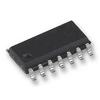
74HC164D NXP Semiconductors, 74HC164D Datasheet

74HC164D
Specifications of 74HC164D
Available stocks
Related parts for 74HC164D
74HC164D Summary of contents
Page 1
Rev. 03 — 4 April 2005 1. General description The 74HC164; 74HCT164 are high-speed Si-gate CMOS devices and are pin compatible with Low power Schottky TTL (LSTTL). They are specified in compliance with ...
Page 2
... For HC the condition is V [3] For HCT the condition Ordering information Table 2: Ordering information Type number Package Temperature range 74HC164N +125 C 74HC164D +125 C 74HC164DB +125 C 74HC164PW +125 C 74HCT164N +125 C 74HCT164D +125 C 9397 750 14693 Product data sheet Quick reference data …continued = ns. ...
Page 3
Philips Semiconductors Table 2: Ordering information Type number Package Temperature range 74HCT164DB +125 C 74HCT164PW +125 C 74HCT164BQ +125 C 5. Functional diagram Fig 1. Logic symbol Fig 3. Logic diagram ...
Page 4
Philips Semiconductors DSA DSB FF1 Fig 4. Functional diagram 6. Pinning information 6.1 Pinning Fig 5. Pin configuration DIP14, SO14, 6.2 Pin description Table 3: Symbol DSA DSB ...
Page 5
Philips Semiconductors Table 3: Symbol GND Functional description 7.1 Function selection Table 4: Operating modes Reset (clear) L Shift [ HIGH voltage level h = HIGH voltage level one ...
Page 6
Philips Semiconductors Table 5: In accordance with the Absolute Maximum Rating System (IEC 60134). Voltages are referenced to GND (ground = 0 V). Symbol P tot [1] For DIP14 packages: P [2] For SO14 packages: P For SSOP14 and TSSOP14 ...
Page 7
Philips Semiconductors Table 7: Static characteristics for 74HC164 At recommended operating conditions; voltages are referenced to GND (ground = 0 V). Symbol Parameter V LOW-level input voltage IL V HIGH-level output voltage OH V LOW-level output voltage OL I input ...
Page 8
Philips Semiconductors Table 7: Static characteristics for 74HC164 At recommended operating conditions; voltages are referenced to GND (ground = 0 V). Symbol Parameter +125 C amb V HIGH-level input voltage IH V LOW-level input voltage ...
Page 9
Philips Semiconductors Table 8: Static characteristics for 74HCT164 At recommended operating conditions; voltages are referenced to GND (ground = 0 V). Symbol Parameter +85 C amb V HIGH-level input voltage IH V LOW-level input voltage ...
Page 10
Philips Semiconductors 11. Dynamic characteristics Table 9: GND = Symbol amb PHL PLH t PHL THL TLH rem max ...
Page 11
Philips Semiconductors Table 9: GND = Symbol +85 C amb PHL PLH t PHL THL TLH rem max ...
Page 12
Philips Semiconductors Table 9: GND = Symbol +125 C amb PHL PLH t PHL THL TLH rem max ...
Page 13
Philips Semiconductors Table 10: GND = Symbol amb PHL PLH t PHL THL TLH rem max ...
Page 14
Philips Semiconductors Table 10: GND = Symbol rem max (1) 74HC164: V Fig 7. Waveforms showing the clock (CP) to output (Qn) propagation delays, the clock 9397 750 14693 ...
Page 15
Philips Semiconductors (1) 74HC164: V Fig 8. Waveforms showing the master reset (MR) pulse width, the master reset to output (1) 74HC164: V Fig 9. Waveforms showing the data set-up and hold times for Dn inputs 9397 750 14693 Product ...
Page 16
Philips Semiconductors Fig 10. Load circuitry for switching times 9397 750 14693 Product data sheet V PULSE GENERATOR Definitions test circuit termination resistance should be equal to output impedance Load capacitance including jig and ...
Page 17
Philips Semiconductors 12. Package outline DIP14: plastic dual in-line package; 14 leads (300 mil pin 1 index 1 DIMENSIONS (inch dimensions are derived from the original mm dimensions UNIT max. min. max. ...
Page 18
Philips Semiconductors SO14: plastic small outline package; 14 leads; body width 3.9 mm; body thickness 1. pin 1 index 1 e DIMENSIONS (inch dimensions are derived from the original mm dimensions) A UNIT ...
Page 19
Philips Semiconductors SSOP14: plastic shrink small outline package; 14 leads; body width 5 pin 1 index 1 e DIMENSIONS (mm are the original dimensions) A UNIT max. 0.21 1.80 mm ...
Page 20
Philips Semiconductors TSSOP14: plastic thin shrink small outline package; 14 leads; body width 4 pin 1 index 1 e DIMENSIONS (mm are the original dimensions) A UNIT max. 0.15 0.95 ...
Page 21
Philips Semiconductors DHVQFN14: plastic dual in-line compatible thermal enhanced very thin quad flat package; no leads; 14 terminals; body 2 0.85 mm terminal 1 index area terminal 1 index area ...
Page 22
Philips Semiconductors 13. Revision history Table 11: Revision history Document ID Release date 74HC_HCT164_3 20050404 • Modifications: The format of this data sheet is redesigned to comply with the current presentation and information standard of Philips Semiconductors • Added SOT762-1 ...
Page 23
Philips Semiconductors 14. Data sheet status [1] Level Data sheet status Product status I Objective data Development II Preliminary data Qualification III Product data Production [1] Please consult the most recently issued data sheet before initiating or completing a design. ...
Page 24
Philips Semiconductors 18. Contents 1 General description . . . . . . . . . . . . . . . . . . . . . . 1 2 Features . . . . . . . . ...


