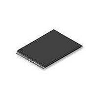
S29GL128P90TFIR10 Spansion Inc., S29GL128P90TFIR10 Datasheet - Page 32

S29GL128P90TFIR10
Manufacturer Part Number
S29GL128P90TFIR10
Description
IC, FLASH, 128MBIT, 90NS, TSOP-56
Manufacturer
Spansion Inc.
Datasheet
1.S29GL128P11TFI020.pdf
(80 pages)
Specifications of S29GL128P90TFIR10
Memory Type
Flash
Memory Size
128Mbit
Memory Configuration
16M X 8 / 8M X 16
Ic Interface Type
CFI, Parallel
Access Time
90ns
Supply Voltage Range
3.0 To 3.6 V
Memory Case Style
TSOP
Data Bus Width
8 bit, 16 bit
Architecture
Sectored
Interface Type
Serial
Supply Voltage (max)
3.6 V
Supply Voltage (min)
3 V
Maximum Operating Current
50 mA
Mounting Style
SMD/SMT
Operating Temperature
+ 85 C
Package / Case
TSOP-56
Lead Free Status / RoHS Status
Lead free / RoHS Compliant
Lead Free Status / RoHS Status
Lead free / RoHS Compliant, Lead free / RoHS Compliant
Available stocks
Company
Part Number
Manufacturer
Quantity
Price
Company:
Part Number:
S29GL128P90TFIR10
Manufacturer:
SPANSION
Quantity:
2 090
Part Number:
S29GL128P90TFIR10
Manufacturer:
SPANSION
Quantity:
20 000
Part Number:
S29GL128P90TFIR10D
Manufacturer:
SPANSION
Quantity:
20 000
32
7.7.4
Chip Erase Command Sequence
Chip erase is a six-bus cycle operation as indicated by
Embedded Erase algorithm, which does not require the system to preprogram prior to erase. The Embedded
Erase algorithm automatically preprograms and verifies the entire memory to an all zero data pattern prior to
electrical erase. After a successful chip erase, all locations of the chip contain FFFFh. The system is not
required to provide any controls or timings during these operations. The
shows the address and data requirements for the chip erase command sequence.
When the Embedded Erase algorithm is complete, that sector returns to the read mode and addresses are no
longer latched. The system can determine the status of the erase operation by using DQ7 or DQ6/DQ2. Refer
to “Write Operation Status” for information on these status bits.
The Unlock Bypass feature allows the host system to send program commands to the Flash device without
first writing unlock cycles within the command sequence. See
function.
Any commands written during the chip erase operation are ignored. However, note that a hardware reset
immediately terminates the erase operation. If that occurs, the chip erase command sequence should be
reinitiated once that sector has returned to reading array data, to ensure the entire array is properly erased.
Software Functions and Sample Code
The following is a C source code example of using the chip erase function. Refer to the Spansion Low Level
Driver User’s Guide (available on www.spansion.com) for general information on Spansion Flash memory
software development guidelines.
Cycle
/* Example: Chip Erase Command */
/* Note: Cannot be suspended
1
2
3
4
5
6
*( (UINT16 *)base_addr + 0x555 ) = 0x00AA;
*( (UINT16 *)base_addr + 0x2AA ) = 0x0055;
*( (UINT16 *)base_addr + 0x555 ) = 0x0080;
*( (UINT16 *)base_addr + 0x555 ) = 0x00AA;
*( (UINT16 *)base_addr + 0x2AA ) = 0x0055;
*( (UINT16 *)base_addr + 0x555 ) = 0x0010;
Chip Erase Command
Setup Command
Description
Unlock
Unlock
Unlock
Unlock
S29GL-P MirrorBit
*/
(LLD Function = lld_ChipEraseCmd)
Operation
Table 7.9 Chip Erase
D a t a
Write
Write
Write
Write
Write
Write
®
Flash Family
/* write unlock cycle 1
/* write unlock cycle 2
/* write setup command
/* write additional unlock cycle 1 */
/* write additional unlock cycle 2 */
/* write chip erase command
S h e e t
Table 12.1 on page
Byte Address
Base + AAAh
Base + AAAh
Base + AAAh
Base + AAAh
Base + 555h
Base + 555h
Section 7.7.8
Command Definitions on page 68
S29GL-P_00_A12 November 20, 2009
Word Address
69. These commands invoke the
Base + 2AAh
Base + 2AAh
Base + 555h
Base + 555h
Base + 555h
Base + 555h
for details on the Unlock Bypass
*/
*/
*/
*/
00AAh
00AAh
0055h
0080h
0055h
0010h
Data


