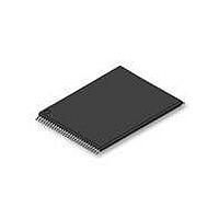
S29GL128P90TFIR10 Spansion Inc., S29GL128P90TFIR10 Datasheet - Page 78

S29GL128P90TFIR10
Manufacturer Part Number
S29GL128P90TFIR10
Description
IC, FLASH, 128MBIT, 90NS, TSOP-56
Manufacturer
Spansion Inc.
Datasheet
1.S29GL128P11TFI020.pdf
(80 pages)
Specifications of S29GL128P90TFIR10
Memory Type
Flash
Memory Size
128Mbit
Memory Configuration
16M X 8 / 8M X 16
Ic Interface Type
CFI, Parallel
Access Time
90ns
Supply Voltage Range
3.0 To 3.6 V
Memory Case Style
TSOP
Data Bus Width
8 bit, 16 bit
Architecture
Sectored
Interface Type
Serial
Supply Voltage (max)
3.6 V
Supply Voltage (min)
3 V
Maximum Operating Current
50 mA
Mounting Style
SMD/SMT
Operating Temperature
+ 85 C
Package / Case
TSOP-56
Lead Free Status / RoHS Status
Lead free / RoHS Compliant
Lead Free Status / RoHS Status
Lead free / RoHS Compliant, Lead free / RoHS Compliant
Available stocks
Company
Part Number
Manufacturer
Quantity
Price
Company:
Part Number:
S29GL128P90TFIR10
Manufacturer:
SPANSION
Quantity:
2 090
Part Number:
S29GL128P90TFIR10
Manufacturer:
SPANSION
Quantity:
20 000
Part Number:
S29GL128P90TFIR10D
Manufacturer:
SPANSION
Quantity:
20 000
78
Revision A8 (November 28, 2007)
Ordering Information
Operating Ranges
Revision A9 (February 15, 2008)
Electrical Specification
Erase and Programming Performance
Sector Protection Command Definition,
x16 Table
Advance Information on S29GL-R 65
nm MirrorBit Hardware Reset (RESET#)
and Power-up Sequence
Revision A10 (March 19, 2008)
Global
DC Characteristics
Sector Protection Command Definitions
(x16 & x8 tables)
Revision A11 (June 11, 2008)
Ordering Information
Figure: Write Operation Status
Flowchart
Revision A12 (November 20, 2009)
Table Input/Output Descriptions
Figure 64-ball Fortified Ball Grid Array
Figure 56-pin Standard TSOP (Top
View)
Table Autoselect Exit
Table Chip Erase
Erase Suspend/Erase Resume
Tables
Unlock Bypass
Writing Commands/Command
Sequence
WP#/ACC Method
Secured Silicon Sector Entry/Exit
Command Sequence
Table Secured Silicon Sector Exit
Figure Test Setup
Table Test Specification
Table S29GL-P Erase and Program
Operations
Table S29GL-P Alternate CE#
Controlled Erase and Program
Operations
Program Suspend
Program Resume
Unlock Bypass Entry
Unlock Bypass Program
Unlock Bypass Reset
Section
New commercial operating temperature option
New operating temperature range
Modified Test Conditions
Chip Program Time: removed comment
Corrected Lock Register “Read” address
Power-Up Sequence Timings Table: modified Note 2 - reduced timing from 500 µs to 300 µs
Changed document status to Full Production.
Changed Max values for Input Load Current (I
Changed Lock Register Read command from “DATA” to “RD”
Revised Commercial temperature range
Updated flowchart
Removed RFU description
Changed all RFU pins to NC pins
Changed all RFU pins to NC pins
Changed cycle description to Auto Select Exit Command
Changed address of last C source code command from 0x000h to 0x555h
Changed first paragraph, second sentence to sector address is “don't care” for Erase Suspend
Changed sixth paragraph, second sentence to sector address is “don't care” for Erase Suspend
Added Byte Address to tables
Third paragraph, first sentence added unlock bypass Sector Erase and unlock bypass Chip Erase
as valid commands
Changed paragraph, third sentence to sector address of exit command is “don't care”.
Changed tables listed in fourth sentence to Table 6.1-6.4
Changed table listed in Note section to 11.2.
Added source code for program under Table 10.3
Changed Byte and Word addresses of Exit Cycle to “XXXh”
Changed test setup to show only a load of CL
Removed Output Load Test Condition
Removed t
Changed description of t
Change Note 2 to “DC Characteristics”
GHWL
S29GL-P MirrorBit
GHEL
D a t a
to (OE# High to CE# Low)
®
Flash Family
S h e e t
Description
LI
)
S29GL-P_00_A12 November 20, 2009


