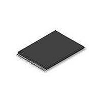
S29GL256P10TFI010 Spansion Inc., S29GL256P10TFI010 Datasheet - Page 27

S29GL256P10TFI010
Manufacturer Part Number
S29GL256P10TFI010
Description
IC, FLASH, 256MBIT, 100NS, TSOP-56
Manufacturer
Spansion Inc.
Specifications of S29GL256P10TFI010
Memory Type
Flash
Memory Size
256Mbit
Memory Configuration
32M X 8 / 16M X 16
Ic Interface Type
CFI, Parallel
Access Time
100ns
Supply Voltage Range
2.7 To 3.6 V
Memory Case Style
TSOP
Data Bus Width
8 bit, 16 bit
Architecture
Uniform
Interface Type
Page-mode
Supply Voltage (max)
3.6 V
Supply Voltage (min)
2.7 V
Maximum Operating Current
50 mA
Mounting Style
SMD/SMT
Operating Temperature
+ 85 C
Package / Case
TSOP-56
Lead Free Status / RoHS Status
Lead free / RoHS Compliant
Lead Free Status / RoHS Status
Lead free / RoHS Compliant, Lead free / RoHS Compliant
Available stocks
Company
Part Number
Manufacturer
Quantity
Price
Company:
Part Number:
S29GL256P10TFI010
Manufacturer:
AD
Quantity:
2 400
Company:
Part Number:
S29GL256P10TFI010
Manufacturer:
SPANSION
Quantity:
5 530
Company:
Part Number:
S29GL256P10TFI010
Manufacturer:
SPANSION
Quantity:
2 890
Company:
Part Number:
S29GL256P10TFI010
Manufacturer:
SAPION
Quantity:
1
Part Number:
S29GL256P10TFI010
Manufacturer:
SPANSION
Quantity:
20 000
November 8, 2007 S29GL-P_00_A7
The write-buffer “embedded” programming operation can be suspended using the standard suspend/resume
commands. Upon successful completion of the Write Buffer Programming operation, the device returns to
READ mode.
The Write Buffer Programming Sequence is ABORTED under any of the following conditions:
The ABORT condition is indicated by DQ1 = 1, DQ7 = DATA# (for the “last address location loaded”), DQ6 =
TOGGLE, DQ5 = 0. This indicates that the Write Buffer Programming Operation was ABORTED. A “Write-to-
Buffer-Abort reset” command sequence is required when using the write buffer Programming features in
Unlock Bypass mode. Note that the Secured Silicon sector, autoselect, and CFI functions are unavailable
when a program operation is in progress.
Write buffer programming is allowed in any sequence of memory (or address) locations. These flash devices
are capable of handling multiple write buffer programming operations on the same write buffer address range
without intervening erases.
Use of the write buffer is strongly recommended for programming when multiple words are to be
programmed.
Load a value that is greater than the page buffer size during the “Number of Locations to Program” step.
Write to an address in a sector different than the one specified during the Write-Buffer-Load command.
Write an Address/Data pair to a different write-buffer-page than the one selected by the “Starting Address”
during the “write buffer data loading” stage of the operation.
Writing anything other than the Program to Buffer Flash Command after the specified number of “data
load” cycles.
D a t a
S h e e t
S29GL-P MirrorBit
( P r e l i m i n a r y )
®
Flash Family
27


