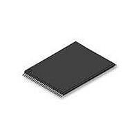
S29GL256P10TFI010 Spansion Inc., S29GL256P10TFI010 Datasheet - Page 69

S29GL256P10TFI010
Manufacturer Part Number
S29GL256P10TFI010
Description
IC, FLASH, 256MBIT, 100NS, TSOP-56
Manufacturer
Spansion Inc.
Specifications of S29GL256P10TFI010
Memory Type
Flash
Memory Size
256Mbit
Memory Configuration
32M X 8 / 16M X 16
Ic Interface Type
CFI, Parallel
Access Time
100ns
Supply Voltage Range
2.7 To 3.6 V
Memory Case Style
TSOP
Data Bus Width
8 bit, 16 bit
Architecture
Uniform
Interface Type
Page-mode
Supply Voltage (max)
3.6 V
Supply Voltage (min)
2.7 V
Maximum Operating Current
50 mA
Mounting Style
SMD/SMT
Operating Temperature
+ 85 C
Package / Case
TSOP-56
Lead Free Status / RoHS Status
Lead free / RoHS Compliant
Lead Free Status / RoHS Status
Lead free / RoHS Compliant, Lead free / RoHS Compliant
Available stocks
Company
Part Number
Manufacturer
Quantity
Price
Company:
Part Number:
S29GL256P10TFI010
Manufacturer:
AD
Quantity:
2 400
Company:
Part Number:
S29GL256P10TFI010
Manufacturer:
SPANSION
Quantity:
5 530
Company:
Part Number:
S29GL256P10TFI010
Manufacturer:
SPANSION
Quantity:
2 890
Company:
Part Number:
S29GL256P10TFI010
Manufacturer:
SAPION
Quantity:
1
Part Number:
S29GL256P10TFI010
Manufacturer:
SPANSION
Quantity:
20 000
November 8, 2007 S29GL-P_00_A7
Legend
X = Don’t care
RD(0) = Read data.
SA = Sector Address. Address bits A
PWD = Password
Notes
1. See
2. All values are in hexadecimal.
3. All bus cycles are write cycles unless otherwise noted.
4. Data bits DQ15-DQ8 are don’t cares for unlock and command cycles.
5. Address bits A
6. All Lock Register bits are one-time programmable. Program state = “0” and
unless SA or PA required. (A
the erase state = “1.” The Persistent Protection Mode Lock Bit and the
Password Protection Mode Lock Bit cannot be programmed at the same
time or the Lock Register Bits Program operation aborts and returns the
device to read mode. Lock Register bits that are reserved for future use
default to “1’s.” The Lock Register is shipped out as “FFFF’s” before Lock
Register Bit program execution.
Command Set Entry
Program
Read
Command Set Exit (7, 8)
Command Set Entry
Password Program
Password Read
Password Unlock
Command Set Exit (7, 8)
PPB Command Set Entry
PPB Program (11, 12)
All PPB Erase
PPB Status Read
PPB Command Set Exit (7, 8)
PPB Lock Command Set Entry
PPB Lock Set
PPB Lock Status Read
PPB Lock Command Set Exit (7, 8)
DYB Command Set Entry
DYB Set (11, 12)
DYB Clear
DYB Status Read
DYB Command Set Exit (7, 8)
Table 7.1 on page 19
Command (Notes)
(6)
(6)
(12)
MAX
(12)
(13)
:A16 are don’t cares for unlock and command cycles,
(10)
(10)
(12)
(12)
(9)
(12)
for description of bus operations.
MAX
is the Highest Address pin.)
max
D a t a
Table 12.2 S29GL-P Sector Protection Command Definitions, x16
–A16 uniquely select any sector.
3
2
1
2
3
2
4
7
2
3
2
2
1
2
3
2
1
2
3
2
2
1
2
S h e e t
First/Seventh
Addr
XXX
XXX
XXX
XXX
XXX
XXX
XXX
XXX
XXX
XXX
XXX
XXX
XXX
555
77h
555
555
555
555
SA
SA
00
00
00
PWD0
RD (0)
RD (0)
RD (0)
S29GL-P MirrorBit
DATA
Data
AA
AA
AA
AA
AA
A0
A0
A0
A0
A0
A0
90
25
29
90
80
90
90
90
( P r e l i m i n a r y )
PWA x
Addr
XXX
XXX
XXX
XXX
XXX
XXX
XXX
2AA
2AA
2AA
2AA
2AA
SA
SA
SA
00
00
01
Second
PWD x
PWD 1
DATA
Data
55
00
55
03
00
55
00
30
00
55
00
00
00
01
00
55
®
PWD
Data = Lock Register Contents: PD(0) = Secured Silicon Sector Protection Bit,
PD(1) = Persistent Protection Mode Lock Bit, PD(2) = Password Protection
Mode Lock Bit.
7. The Exit command returns the device to reading the array.
8. If any Command Set Entry command was written, an Exit command must
9. For PWDx, only one portion of the password can be programmed per each
10. Note that the password portion can be entered or read in any order as long
11. If ACC = V
12. Protected State = “00h,” Unprotected State = “01h.”
13. The All PPB Erase command embeds programming of all PPB bits before
Flash Family
be issued to reset the device into read mode.
“A0” command.
as the entire 64-bit password is entered or read.
erasure.
x
Addr
555
555
555
555
555
= Password word0, word1, word2, and word3.
02
00
Bus Cycles (Notes 1–5)
Third
PWD 2
PWD 0
HH
Data
C0
E0
40
60
50
, sector protection matches when ACC = V
Addr
03
01
Fourth
PWD 3
PWD 1
Data
Addr
02
Fifth
PWD 2
Data
IH
.
Addr
03
Sixth
PWD 3
Data
69


