IS61LV25616AL-10TL INTEGRATED SILICON SOLUTION (ISSI), IS61LV25616AL-10TL Datasheet
IS61LV25616AL-10TL
Specifications of IS61LV25616AL-10TL
Available stocks


Related parts for IS61LV25616AL-10TL


IS61LV25616AL-10TL Summary of contents
Page 1
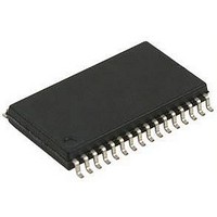
... Output Enable inputs, CE and OE. The active LOW Write Enable (WE) controls both writing and reading of the memory. A data byte allows Upper Byte (UB) and Lower Byte (LB) access. The IS61LV25616AL is packaged in the JEDEC standard 44-pin 400-mil SOJ, 44-pin TSOP Type II, 44-pin LQFP and 48-pin Mini BGA (8mm x 10mm). 256K x 16 ...
Page 2
... IS61LV25616AL TRUTH TABLE Mode Not Selected X H Output Disabled Read Write PIN CONFIGURATIONS 44-Pin TSOP (Type II) and SOJ I/O0 7 I/O1 8 I/O2 9 I/O3 10 VDD 11 GND 12 I/O4 13 I/O5 14 I/ I/O0-I/ High High High OUT High OUT High PIN DESCRIPTIONS A0-A17 I/O0-I/O15 CE 44 ...
Page 3
... IS61LV25616AL PIN CONFIGURATIONS 44-Pin LQFP I/ I/O1 4 I/O2 5 I/O3 TOP VIEW 6 VDD 7 GND 8 I/O4 9 I/O5 10 I/ PIN DESCRIPTIONS A0-A17 Address Inputs I/O0-I/O15 Data Inputs/Outputs CE Chip Enable Input OE Output Enable Input WE Write Enable Input LB Lower-byte Control (I/O0-I/O7) UB Upper-byte Control (I/O8-I/O15 Connection V Power ...
Page 4
... IS61LV25616AL ABSOLUTE MAXIMUM RATINGS Symbol Parameter V Terminal Voltage with Respect to GND TERM T Storage Temperature STG P Power Dissipation T Note: 1. Stress greater than those listed under ABSOLUTE MAXIMUM RATINGS may cause permanent damage to the device. This is a stress rating only and functional operation of the device at these or any other conditions above those indicated in the operational sections of this specification is not implied ...
Page 5
... IS61LV25616AL POWER SUPPLY CHARACTERISTICS Symbol Parameter Test Conditions I V Dynamic Operating Supply Current I OUT I TTL Standby Current (TTL Inputs ≥ TTL Standby Current (TTL Inputs ≥ CMOS Standby ≥ V Current (CMOS Inputs Note address and data inputs are cycling at the maximum frequency means no input lines change. ...
Page 6
... IS61LV25616AL READ CYCLE SWITCHING CHARACTERISTICS Symbol Parameter t Read Cycle Time RC t Address Access Time AA t Output Hold Time OHA CE Access Time t ACE OE Access Time t DOE OE to High-Z Output t (2) HZOE OE to Low-Z Output t (2) LZOE CE to High-Z Output t (2 HZCE CE to Low-Z Output ...
Page 7
... IS61LV25616AL AC WAVEFORMS (1,2) (Address Controlled) ( READ CYCLE NO. 1 ADDRESS D OUT PREVIOUS DATA VALID (1,3) READ CYCLE NO. 2 ADDRESS LZCE LB LZB HIGH-Z D OUT V DD Supply Current Notes HIGH for a Read Cycle. 2. The device is continuously selected. OE, CE, UB Address is valid prior to or coincident with CE LOW transition. ...
Page 8
... IS61LV25616AL (1,3) READ CYCLE NO. 2 ADDRESS LZCE LB LZB HIGH-Z D OUT V DD Supply Current Notes HIGH for a Read Cycle. 2. The device is continuously selected. OE, CE, UB Address is valid prior to or coincident with CE LOW transition. WRITE CYCLE SWITCHING CHARACTERISTICS Symbol Parameter t Write Cycle Time Write End ...
Page 9
... IS61LV25616AL AC WAVEFORMS (CE Controlled HIGH or LOW) WRITE CYCLE NO. 1 ADDRESS UB DATA UNDEFINED OUT D IN Notes: 1. WRITE is an internally generated signal asserted during an overlap of the LOW states on the CE and WE inputs and at least one of the LB and UB inputs being in the LOW state WRITE = (CE) (LB) = (UB) (WE) ...
Page 10
... IS61LV25616AL AC WAVEFORMS (WE Controlled LOW During Write Cycle) WRITE CYCLE NO. 3 ADDRESS LOW OE CE LOW UB DATA UNDEFINED OUT D IN WRITE CYCLE NO. 4 (LB, UB Controlled, Back-to-Back Write) ADDRESS OE CE LOW WE UB HZWE D OUT DATA UNDEFINED D IN Notes: 1. The internal Write time is defined by the overlap LOW, UB and/ LOW, and WE = LOW. All signals must be in valid states to initiate a Write, but any can be deasserted to terminate the Write ...
Page 11
... IS61LV25616AL DATA RETENTION SWITCHING CHARACTERISTICS Symbol Parameter V V for Data Retention Data Retention Current DR t Data Retention Setup Time SDR t Recovery Time RDR Note 1: Typical values are measured DATA RETENTION WAVEFORM V DD 1.65V 1. GND Integrated Silicon Solution, Inc. — www.issi.com — ...
Page 12
... Commercial Range: 0°C to +70°C Speed (ns) Order Part No. 10 IS61LV25616AL-10T IS61LV25616AL-10TL IS61LV25616AL-10K 12 IS61LV25616AL-12T Industrial Range: –40°C to +85°C Speed (ns) Order Part No. 10 IS61LV25616AL-10TI IS61LV25616AL-10TLI IS61LV25616AL-10KI IS61LV25616AL-10KLI IS61LV25616AL-10LQI IS61LV25616AL-10BI IS61LV25616AL-10BLI 12 IS61LV25616AL-12TI 12 Package TSOP (Type II) TSOP (Type II), Lead-free 400-mil SOJ TSOP (Type II) ...
Page 13
PACKAGING INFORMATION LQFP (Low Profile Quad Flat Pack) Package Code: LQ (44-pin Low Profile Quad Flat Pack (LQ) Ref. Std. No. Leads Millimeters Symbol Min Max A — 1.60 A1 0.05 0.15 A2 1.35 1.45 ...
Page 14
PACKAGING INFORMATION 400-mil Plastic SOJ Package Code Millimeters Inches Symbol Min Max Min No. Leads ( 3.25 3.75 0.128 0.148 A1 0.64 — 0.025 A2 2.08 — 0.082 B 0.38 0.51 0.015 0.020 ...
Page 15
PACKAGING INFORMATION Millimeters Inches Symbol Min Max Min No. Leads ( 3.25 3.75 0.128 0.148 A1 0.64 — 0.025 A2 2.08 — 0.082 B 0.38 0.51 0.015 0.020 b 0.66 0.81 0.026 0.032 C 0.18 0.33 0.007 0.013 ...
Page 16
PACKAGING INFORMATION Mini Ball Grid Array Package Code: B (48-pin) Top View SEATING PLANE mBGA - 6mm x 8mm MILLIMETERS Sym. Min. Typ. Max. Min. Typ. ...
Page 17
PACKAGING INFORMATION Plastic TSOP Package Code: T (Type II Millimeters Inches Symbol Min Max Min Ref. Std. No. Leads ( — 1.20 — A1 0.05 0.15 0.002 0.006 b 0.30 0.52 0.012 ...