TEA1751LT/N1 NXP Semiconductors, TEA1751LT/N1 Datasheet
TEA1751LT/N1
Specifications of TEA1751LT/N1
Available stocks


Related parts for TEA1751LT/N1


TEA1751LT/N1 Summary of contents
Page 1
TEA1751T; TEA1751LT GreenChip III SMPS control IC Rev. 02 — 23 December 2009 1. General description The GreenChip III is the third generation of green Switched Mode Power Supply (SMPS) controller ICs. The TEA1751(L)T (TEA1751T and TEA1751LT) combines a controller ...
Page 2
... NXP Semiconductors 2.3 PFC green features Valley/zero voltage switching for minimum switching losses (NXP patented). Frequency limitation to reduce switching losses. PFC is switched off when a low load is detected at the flyback output. 2.4 Flyback green features Valley switching for minimum switching losses (NXP patented). ...
Page 3
... NXP Semiconductors 5. Block diagram 1.12 V 3.5 V LOW VIN VINSENSE 7 BOOST LATCH RESET PFCCOMP 6 LOW POWER VOSENSE 9 2. μA BOOST LOW VIN VoOVP VoSTART FB VoSHORT OCP BLANK 500 mV PFCSENSE 11 60 μA SOFT START TIMER 4 μs VALLEY DETECT PFCAUX 8 TIMER 50 μs 100 mV Remark: For the TEA1751L the time-out is latched ...
Page 4
... NXP Semiconductors 6. Pinning information 6.1 Pinning Fig 2. Pin configuration: TEA1751(L)T (SOT109-1) 6.2 Pin description Table 2. Symbol V CC GND FBCTRL FBAUX LATCH PFCCOMP VINSENSE PFCAUX VOSENSE FBSENSE PFCSENSE PFCDRIVER FBDRIVER HVS HV TEA1751T_LT_2 Product data sheet TEA1751T; TEA1751LT GND FBCTRL 3 4 FBAUX TEA1751(L)T ...
Page 5
... NXP Semiconductors 7. Functional description 7.1 General control The TEA1751(L)T contains a controller for a power factor correction circuit as well as a controller for a flyback circuit. A typical configuration is shown in Fig 3. Typical configuration 7.1.1 Start-up and UnderVoltage LockOut (UVLO) Initially the capacitor on the V As long shorted to ground. For a short start-up time the charge current above V ...
Page 6
... NXP Semiconductors As soon as the flyback converter is started, the voltage on the FBCTRL pin is monitored. If the output voltage of the flyback converter does not reach its intended regulation level in a predefined time, the voltage on the FBCTRL pin reaches the V is assumed. The TEA1751 then initiates a safe restart, while in the TEA1751L the protection is latched ...
Page 7
... NXP Semiconductors VINSENSE LATCH PROTECTION PFCSENSE PFCDRIVER FBSENSE FBDRIVER FBCTRL VOSENSE Fig 4. Start-up sequence, normal operation and restart sequence 7.1.2 Supply management All internal reference voltages are derived from a temperature compensated and trimmed on-chip band gap circuit. Internal reference currents are derived from a temperature compensated and trimmed on-chip current reference circuit ...
Page 8
... NXP Semiconductors 7.1.4 Fast latch reset In a typical application the mains can be interrupted briefly to reset the latched protection. The PFC bus capacitor, C reset. Typically the PFC bus capacitor, C level. When the latched protection is set, the clamping circuit of the VINSENSE circuit is disabled. (see also 750 mV (typical) and after that is raised to 870 mV (typical), the latched protection is reset ...
Page 9
... NXP Semiconductors 7.2.3 Frequency limitation To optimize the transformer and minimize switching losses, the switching frequency is limited to f limit, the system switches over to discontinuous conduction mode. Also here, the PFC MOSFET is only switched minimum voltage across the switch (valley switching). 7.2.4 Mains voltage compensation (VINSENSE pin) The mathematical equation for the transfer function of a power factor corrector contains the square of the mains input voltage ...
Page 10
... NXP Semiconductors Fig 5. Soft start-up of PFC 7.2.6 Low power mode When the output power of the flyback converter (see converter switches over to frequency reduction mode. When frequency reduction mode is entered by the flyback controller, the power factor correction circuit is switched off to maintain high efficiency. ...
Page 11
... NXP Semiconductors Fig 6. Voltage to current transfer function for dual boost PFC 7.2.8 Overcurrent protection (PFCSENSE pin) The maximum peak current is limited cycle-by-cycle by sensing the voltage across an external sense resistor, R measured via the PFCSENSE pin. 7.2.9 Mains undervoltage lockout / brownout protection (VINSENSE pin) To prevent the PFC from operating at very low mains input voltages, the voltage on the VINSENSE pin is sensed continuously ...
Page 12
... NXP Semiconductors 7.3 Flyback controller The TEA1751(L)T includes a controller for a flyback converter. The flyback converter operates in quasi-resonant or discontinuous conduction mode with valley switching. The auxiliary winding of the flyback transformer provides demagnetization detection and powers the IC after start-up. 7.3.1 Multimode operation The TEA1751(L)T flyback controller can operate in several modes; see switching frequency Fig 7 ...
Page 13
... NXP Semiconductors switching frequency Fig 8. Frequency control of flyback part 7.3.2 Valley switching (HV pin) Refer to Figure on-time (determined by the FBSENSE voltage and the FBCTRL voltage), the MOSFET is switched off and the secondary stroke starts. After the secondary stroke, the drain voltage shows an oscillation with a frequency of approximately the primary self-inductance of the flyback transformer and C drain node ...
Page 14
... NXP Semiconductors (1) Start of new cycle at lowest drain voltage. (2) Start of new cycle in a classical Pulse Width Modulation (PWM) system without valley detection. Fig 9. Signals for valley switching 7.3.3 Current mode control (FBSENSE pin) Current mode control is used for the flyback converter for its good line regulation. ...
Page 15
... NXP Semiconductors Fig 10. Peak current control of flyback part The driver output is latched in the logic, preventing multiple switch-on. 7.3.4 Demagnetization (FBAUX pin) The system is always in quasi-resonant or discontinuous conduction mode. The internal oscillator does not start a new primary stroke until the previous secondary stroke has ended ...
Page 16
... NXP Semiconductors In normal operating conditions, when the converter is regulating the output voltage, the voltage on the FBCTRL pin is between 1.4 V and 2.0 V (typical values) from minimum to maximum output power. Fig 11. Time-out protection circuit Fig 12. Time-out protection (signals), safe restart in the TEA1751 Fig 13. Time-out protection (signals), latched in the TEA1751L ...
Page 17
... NXP Semiconductors 7.3.6 Soft start-up (pin FBSENSE) To prevent audible transformer noise during start-up, the transformer peak current, I slowly increased by the soft start function. This can be achieved by inserting a resistor and a capacitor between pin 10, FBSENSE, and the current sense resistor. An internal current source charges the capacitor approximately 0 ...
Page 18
... NXP Semiconductors subsequent OVP events are detected, the IC assumes a true OVP and the OVP circuit switches the power MOSFET off. As the protection is latched, the converter only restarts after the internal latch is reset typical application the mains should be interrupted to reset the internal latch. ...
Page 19
... NXP Semiconductors Fig 16. Overpower protection curve 7.3.11 Driver (pin FBDRIVER) The driver circuit to the gate of the external power MOSFET has a current sourcing capability of typically −500 mA and a current sink capability of typically 1.2 A. This permits fast turn-on and turn-off of the power MOSFET for efficient operation. ...
Page 20
... NXP Semiconductors Table 3. In accordance with the Absolute Maximum Rating System (IEC 60134). Symbol I PFCDRIVER I HV General P tot T stg T j ESD V ESD [1] Equivalent to discharging a 100 pF capacitor through a 1.5 kΩ series resistor. Equivalent to discharging a 200 pF capacitor through a 0.75 μH coil and a 10 Ω resistor. ...
Page 21
... NXP Semiconductors Table 5. Characteristics …continued ° all voltages are measured with respect to ground (pin 2); currents are positive when flowing into amb CC the IC; unless otherwise specified. Symbol Parameter V undervoltage lockout threshold th(UVLO) voltage V hysteresis of start voltage start(hys) V hysteresis voltage hys I low charging current ...
Page 22
... NXP Semiconductors Table 5. Characteristics …continued ° all voltages are measured with respect to ground (pin 2); currents are positive when flowing into amb CC the IC; unless otherwise specified. Symbol Parameter Output voltage sensing PFC (pin VOSENSE) V open-loop threshold voltage on th(ol)(VOSENSE) pin VOSENSE V regulation voltage on pin ...
Page 23
... NXP Semiconductors Table 5. Characteristics …continued ° all voltages are measured with respect to ground (pin 2); currents are positive when flowing into amb CC the IC; unless otherwise specified. Symbol Parameter I sink current on pin sink(PFCDRIVER) PFCDRIVER V maximum output voltage on pin O(PFCDRIVER)max PFCDRIVER Overvoltage protection flyback (pin FBAUX) ...
Page 24
... NXP Semiconductors Table 5. Characteristics …continued ° all voltages are measured with respect to ground (pin 2); currents are positive when flowing into amb CC the IC; unless otherwise specified. Symbol Parameter t valley recognition to switch-on d(vrec-swon) delay time Soft start flyback (pin FBSENSE) I flyback soft start current ...
Page 25
... NXP Semiconductors 11. Application information A power supply with the TEA1751(L)T consists of a power factor correction circuit followed by a flyback converter. See Capacitor C rectified mains during start-up and via the auxiliary winding of the flyback converter during operation. Sense resistors R MOSFETs S1 and S2 into a voltage at pins PFCSENSE and FBSENSE. The values of ...
Page 26
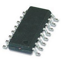
... NXP Semiconductors 12. Package outline SO16: plastic small outline package; 16 leads; body width 3 pin 1 index 1 e DIMENSIONS (inch dimensions are derived from the original mm dimensions) A UNIT max. 0.25 1.45 mm 1.75 0.25 0.10 1.25 0.010 0.057 inches 0.069 0.01 0.004 0.049 Note 1. Plastic or metal protrusions of 0.15 mm (0.006 inch) maximum per side are not included. ...
Page 27
... NXP Semiconductors 13. Revision history Table 6. Revision history Document ID Release date TEA1751T_LT_2 20091223 • Modifications: Value for junction temperature (T TEA1751T_LT_1 20090210 TEA1751T_LT_2 Product data sheet TEA1751T; TEA1751LT Data sheet status Change notice Product data sheet - ) changed in Table j Product data sheet - Rev. 02 — 23 December 2009 ...
Page 28
... Right to make changes — NXP Semiconductors reserves the right to make changes to information published in this document, including without limitation specifications and product descriptions, at any time and without notice ...
Page 29
... NXP Semiconductors 16. Contents 1 General description . . . . . . . . . . . . . . . . . . . . . . 1 2 Features . . . . . . . . . . . . . . . . . . . . . . . . . . . . . . . 1 2.1 Distinctive features . . . . . . . . . . . . . . . . . . . . . . 1 2.2 Green features . . . . . . . . . . . . . . . . . . . . . . . . . 1 2.3 PFC green features . . . . . . . . . . . . . . . . . . . . . 2 2.4 Flyback green features . . . . . . . . . . . . . . . . . . . 2 2.5 Protection features . . . . . . . . . . . . . . . . . . . . . . 2 3 Applications . . . . . . . . . . . . . . . . . . . . . . . . . . . . 2 4 Ordering information . . . . . . . . . . . . . . . . . . . . . 2 5 Block diagram . . . . . . . . . . . . . . . . . . . . . . . . . . 3 6 Pinning information . . . . . . . . . . . . . . . . . . . . . . 4 6.1 Pinning . . . . . . . . . . . . . . . . . . . . . . . . . . . . . . . 4 6.2 Pin description . . . . . . . . . . . . . . . . . . . . . . . . . 4 7 Functional description . . . . . . . . . . . . . . . . . . . 5 7 ...