LM22677TJ-ADJ National Semiconductor, LM22677TJ-ADJ Datasheet
LM22677TJ-ADJ
Specifications of LM22677TJ-ADJ
Available stocks


Related parts for LM22677TJ-ADJ

LM22677TJ-ADJ Summary of contents
Page 1
... The LM22677 series also has built in thermal shut- down, current limiting and an enable control input that can power down the regulator to a low 25 µA quiescent current standby condition. Simplified Application Schematic © 2008 National Semiconductor Corporation Features ■ Wide input voltage range: 4.5V to 42V ■ ...
Page 2
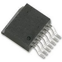
... Connection Diagram Ordering Information Output Voltage Order Number ADJ LM22677TJE-ADJ ADJ LM22677TJ-ADJ 5.0 LM22677TJE-5.0 5.0 LM22677TJ-5.0 Pin Descriptions Pin Name Description 1 SW Switch pin 2 VIN Source input voltage 3 BOOT Bootstrap input 4 GND System ground 5 RT/SYNC Oscillator frequency adjust pin or frequency synchronization ...
Page 3
... Absolute Maximum Ratings If Military/Aerospace specified devices are required, please contact the National Semiconductor Sales Office/ Distributors for availability and specifications. VIN to GND EN Pin Voltage RT/SYNC Pin Voltage SW to GND (Note 2) BOOT Pin Voltage FB Pin Voltage Power Dissipation Junction Temperature Electrical Characteristics junction temperature (T ) range of -40° ...
Page 4
Note 1: Absolute Maximum Ratings indicate limits beyond which damage to the device may occur, including inoperability and degradation of device reliability and/or performance. Functional operation of the device and/or non-degradation at the Absolute Maximum Ratings or other conditions beyond ...
Page 5
Feedback Bias Current vs Temperature Standby Quiescent Current vs Input Voltage Normalized Feedback Voltage vs Input Voltage Normalized Enable Threshold Voltage vs Temperature 30074105 Normalized Feedback Voltage vs Temperature 30074106 Switching Frequency vs RT/SYNC Resistor 30074109 5 30074110 30074107 30074113 ...
Page 6
Typical Application Circuit and Block Diagram www.national.com FIGURE 1. 3. 600 kHz OUT 6 30074114 ...
Page 7
Detailed Operating Description The LM22677 switching regulator features all of the functions necessary to implement an efficient high voltage buck regu- lator using a minimum of external components. This easy to use regulator integrates a 42V N-Channel switch with an ...
Page 8
Soft-Start The soft-start feature allows the regulator to gradually reach the initial steady state operating point, thus reducing start-up stresses and surges. The soft-start is fixed to 500 µs (typical) start-up time and cannot be modified. Switching Frequency Setting and ...
Page 9
The typical location of the internal compensation poles and zeros as well as the DC gain is given in Table 1. ...
Page 10
L If the switching frequency is set higher than 500 kHz, the ca- pacitance value may not be reduced accordingly due to sta- bility requirements. The internal compensation is optimized for circuits with ...
Page 11
Circuit Board Layout Board layout is critical for switching power supplies. First, the ground plane area must be sufficient for thermal dissipation purposes. Second, appropriate guidelines must be followed to reduce the effects of switching noise. Switch mode con- verters ...
Page 12
PCB Layout Example www.national.com 12 30074125 ...
Page 13
Schematic for Buck/Boost (Inverting) Application See AN-1888 for more information on the inverting (buck- boost) application generating a negative output voltage from a positive input voltage. 30074126 13 www.national.com ...
Page 14
Physical Dimensions www.national.com inches (millimeters) unless otherwise noted 7-Lead Plastic TO-263 THIN Package NS Package Number TJ7A 14 ...
Page 15
Notes 15 www.national.com ...
Page 16
... For more National Semiconductor product information and proven design tools, visit the following Web sites at: Products Amplifiers www.national.com/amplifiers Audio www.national.com/audio Clock Conditioners www.national.com/timing Data Converters www.national.com/adc Displays www.national.com/displays Ethernet www.national.com/ethernet Interface www.national.com/interface LVDS www.national.com/lvds Power Management www.national.com/power Switching Regulators www.national.com/switchers LDOs www ...