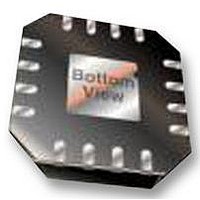
ADL5604ACPZ-R7 Analog Devices Inc, ADL5604ACPZ-R7 Datasheet - Page 20

ADL5604ACPZ-R7
Manufacturer Part Number
ADL5604ACPZ-R7
Description
IC RF AMP, 12.2DB 2700MHZ 5.25V LFCSP-16
Manufacturer
Analog Devices Inc
Datasheet
1.ADL5604ACPZ-R7.pdf
(24 pages)
Specifications of ADL5604ACPZ-R7
Frequency Range
700MHz To 2700MHz
Noise Figure Typ
4.6dB
Power Dissipation Pd
3.9W
Supply Current
318mA
Gain
12.2dB
Rf Type
Broadband, Cellular, Satellite
Current - Supply
318mA
Frequency
700MHz ~ 2.7GHz
Noise Figure
4.6dB
P1db
29.1dBm
Package / Case
16-VQFN, CSP Exposed Pad
Test Frequency
2.63GHz
Voltage - Supply
4.75 V ~ 5.25 V
Rohs Compliant
Yes
Lead Free Status / RoHS Status
Lead free / RoHS Compliant
Other names
ADL5604ACPZ-R7
ADL5604ACPZ-R7TR
ADL5604ACPZ-R7TR
Available stocks
Company
Part Number
Manufacturer
Quantity
Price
Company:
Part Number:
ADL5604ACPZ-R7
Manufacturer:
NICHICON
Quantity:
54 000
ADL5604
EVALUATION BOARD
The schematic of the ADL5604 evaluation board is shown in
Figure 43. This evaluation board uses 25 mils wide, 50 Ω traces
and is made from IS410 material, with a 23mils gap to ground.
The evaluation board is tuned for operation at 2140 MHz. The
inputs and outputs should be ac-coupled with appropriately
sized capacitors; therefore, for low frequency applications, C1
and C2 may need to be increased. DC bias is provided to the
output stage via an inductor connected to the RFOUT pin. A
bias voltage of 5 V is recommended. The evaluation board has a
short non 50 Ω line on its output to accommodate the four
output pins and allow for easier low inductance output matching.
The pads for Pin 9 to Pin 12 are included on this microstrip line
RFIN
NOTES
1. THE COMPONENTS CONTAINED INSIDE THE DASHED BOX ARE ONLY REQUIRED IF IT IS
DESIRED TO POWER DOWN THE ADL5604.
VBIAS
C1
0Ω
NOTE 1
VBIAS
1.3pF
OPEN
10nF
0.1µF
C3
C11
C12
0Ω
R6
R3
0.1µF
C14
R4 OPEN
0.1µF
C15
C4
2.7pF
10nF
0.1µF
C10
C9
R2
0Ω
+VS
–VS
U2
301Ω
AD8009
R1
R8
0Ω
Figure 43. Evaluation Board, 2140 MHz
R5
0Ω
1
2
3
4
VCC2
RFIN
RFIN
VBIAS
VCC2
GND GND GND GND
GND GND GND GND
Rev. A | Page 20 of 24
GND1
16
5
ADL5604
15
6
GND2
14
7
RFOUT
RFOUT
RFOUT
RFOUT
13
8
and are included in all matches. Figure 46 shows the close-up
image of the recommended output pad. The evaluation board
also has hash marks close to the input and output of the
ADL5604, separated by 40 mils. The hash mark closest to the
input is 127 mils from the chip, and the hash mark closest to the
output is 20 mils from the chip.
U2 and its associated circuitry are required only if it is desired
to power down the ADL5604. On the evaluation board, it is
necessary to remove R2 and install a 0 Ω resistor in the R4
position to enable this feature.
GND3
11
10
12
9
R10
R9
0Ω
0Ω
VCC1
L1
16nH
0.1µF
10nF
10µF
C6
C7
C8
2.4pF
L2
OPEN
C5
22pF
C2
RFOUT


