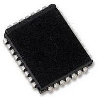
CAT28F010GI-12 CATALYST SEMICONDUCTOR, CAT28F010GI-12 Datasheet

CAT28F010GI-12
Specifications of CAT28F010GI-12
Available stocks
Related parts for CAT28F010GI-12
CAT28F010GI-12 Summary of contents
Page 1
Megabit CMOS Flash Memory FEATURES Fast read access time: 90/120 ns Low power CMOS dissipation: –Active max (CMOS/TTL levels) –Standby max (TTL levels) –Standby: 100 A max (CMOS levels) High speed programming: –10 s per ...
Page 2
CAT28F010 PIN CONFIGURATION DIP Package ( PLCC Package ( N ...
Page 3
ABSOLUTE MAXIMUM RATINGS* Temperature Under Bias .................. - +130 C Storage Temperature ........................ - +150 C Voltage on Any Pin with (1) Respect to Ground ............ -2. Voltage on Pin A with 9 (1) ...
Page 4
CAT28F010 D.C. OPERATING CHARACTERISTICS V = +5V 10%, unless otherwise specified. CC Symbol Parameter I Input Leakage Current LI I Output Leakage Current Standby Current CMOS SB1 Standby Current TTL SB2 ...
Page 5
SUPPLY CHARACTERISTICS Symbol V V Supply Voltage During Read Operations PPL During Read/Erase/Program PPH PP A.C. CHARACTERISTICS, Read Operation V = +5V 10%, unless otherwise specified. CC JEDEC Standard Symbol Symbol Parameter t ...
Page 6
CAT28F010 A.C. CHARACTERISTICS, Program/Erase Operation V = +5V 10%, unless otherwise specified. CC \JEDEC Standard Symbol Symbol Parameter t t Write Cycle Time AVAV Address Setup Time AVWL Address Hold Time WLAX AH t ...
Page 7
FUNCTION TABLE Mode CE Read V IL Output Disable V IL Standby V IH Signature (MFG Signature (Device Program/Erase V IL Write Cycle V IL Read Cycle V IL WRITE COMMAND TABLE Commands are written ...
Page 8
CAT28F010 READ OPERATIONS Read Mode A Read operation is performed with both CE and OE low and with WE high. V can be either high or low, PP however high, the Set READ command has to PP ...
Page 9
WRITE OPERATIONS The following operations are initiated by observing the sequence specified in the Write Command Table. Read Mode The device can be put into a standard READ mode by initiating a write cycle with 00H on the data bus. ...
Page 10
CAT28F010 (1) Figure 5. Chip Erase Algorithm START ERASURE APPLY V PPH PROGRAM ALL BYTES TO 00H INITIALIZE ADDRESS INITIALIZE PLSCNT = 0 WRITE ERASE SETUP COMMAND WRITE ERASE COMMAND TIME OUT 10ms WRITE ERASE VERIFY COMMAND TIME OUT 6 ...
Page 11
Erase Mode During the first Write cycle, the command 20H is written into the command register. In order to commence the erase operation, the identical command of 20H has to be written again into the register. This two-step process ensures ...
Page 12
CAT28F010 Figure 7. Programming Algorithm START PROGRAMMING APPLY V PPH INITIALIZE ADDRESS PLSCNT = 0 WRITE SETUP PROG. COMMAND WRITE PROG. CMD ADDR AND DATA TIME OUT 10 s WRITE PROGRAM VERIFY COMMAND TIME OUT 6 s READ DATA FROM ...
Page 13
Program-Verify Mode A Program-verify cycle is performed to ensure that all bits have been correctly programmed following each byte programming operation. The specific address is already latched from the write cycle just completed, and stays latched until the verify is ...
Page 14
CAT28F010 A.C. CHARACTERISTICS, Read Operation V = +5V 10%, unless otherwise specified. CC JEDEC Standard Symbol Symbol Parameter t t Write Cycle Time AVAV Address Setup Time AVEL Address Hold Time ELAX AH t ...
Page 15
EXAMPLE OF ORDERING INFORMATION Prefix Device # CAT 28F010 Product Number Optional Company ID ORDERING INFORMATION ...
Page 16
CAT28F010 REVISION HISTORY Date Revision Description 01-Jul-04 D Added Green Packages in all areas. 15-Oct-08 E Eliminate PDIP SnPb package. 17-Nov-08 F Change logo and fine print to ON Semiconductor 31-Jul-09 G Update Absolute Maximum Ratings Update Example of Ordering ...


