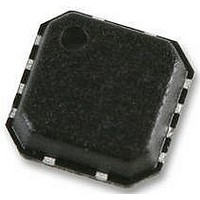
AD8353ACPZ Analog Devices Inc, AD8353ACPZ Datasheet

AD8353ACPZ
Specifications of AD8353ACPZ
Available stocks
Related parts for AD8353ACPZ
AD8353ACPZ Summary of contents
Page 1
FEATURES Fixed gain Operational frequency of 1 MHz to 2.7 GHz Linear output power dBm Input/output internally matched to 50 Ω Temperature and power supply stable Noise figure: 5.3 dB Power supply ...
Page 2
AD8353 TABLE OF CONTENTS Features .............................................................................................. 1 Applications....................................................................................... 1 Functional Block Diagram .............................................................. 1 General Description ......................................................................... 1 Revision History ............................................................................... 2 Specifications..................................................................................... 3 Absolute Maximum Ratings............................................................ 5 ESD Caution.................................................................................. 5 Pin Configuration and Function Descriptions............................. 6 REVISION HISTORY 12/05—Rev. ...
Page 3
SPECIFICATIONS 25°C, 100 nH external inductor between RFOUT and VPOS Table 1. Parameter OVERALL FUNCTION Frequency Range Gain Delta Gain Gain Supply Sensitivity Reverse Isolation ( INPUT INTERFACE ...
Page 4
AD8353 25°C, no external inductor between RFOUT and VPOS Table 2. Parameter OVERALL FUNCTION Frequency Range Gain Delta Gain Gain Supply Sensitivity Reverse Isolation ( INPUT INTERFACE Input ...
Page 5
ABSOLUTE MAXIMUM RATINGS Table 3. Parameter Supply Voltage, VPOS Input Power (re: 50 Ω) Equivalent Voltage Internal Power Dissipation Paddle Not Soldered Paddle Soldered θ (Paddle Soldered) JA θ (Paddle Not Soldered) JA Maximum Junction Temperature Operating Temperature Range Storage ...
Page 6
AD8353 PIN CONFIGURATION AND FUNCTION DESCRIPTIONS Table 4. Pin Function Descriptions Pin No. Mnemonic 1, 8 COM1 RFIN 4, 5 COM2 6 VPOS 7 RFOUT COM1 COM1 1 8 AD8353 NC RFOUT 2 7 TOP VIEW RFIN ...
Page 7
TYPICAL PERFORMANCE CHARACTERISTICS 90 120 150 180 210 240 270 Figure 3. S vs. Frequency 25°C, dc ≤ f ≤ 3 GHz GAIN AT 3. GAIN AT ...
Page 8
AD8353 3.0V 1dB 500 1000 1500 FREQUENCY (MHz) Figure 9. P vs. Frequency 2 and 3 1dB ...
Page 9
NF AT 3.3V 6.0 5 3.0V 4.5 4.0 0 500 1000 1500 2000 FREQUENCY (MHz) Figure 15. Noise Figure vs. Frequency 2 and 3.3 V, ...
Page 10
AD8353 GAIN AT 5.0V GAIN AT 4. 500 1000 1500 2000 FREQUENCY (MHz) Figure 21. Gain vs. Frequency 4 and 5 –5 –10 –15 ...
Page 11
OUTPUT 1dB COMPRESSION POINT (dBm) Figure 27. Distribution 1dB ...
Page 12
AD8353 6.10 6.15 6.20 6.25 6.30 6.35 6.40 6.45 6.50 NOISE FIGURE (dB) Figure 33. Distribution of Noise Figure 5. ...
Page 13
THEORY OF OPERATION The AD8353 is a 2-stage, feedback amplifier employing both shunt-series and shunt-shunt feedback. The first stage is degenerated and resistively loaded and provides approximately gain. The second stage is a PNP-NPN Darlington output stage, ...
Page 14
AD8353 APPLICATIONS The AD8353 RF gain block can be used as a general-purpose, fixed gain amplifier in a wide variety of applications, such as a driver for a transmitter power amplifier (see Figure 37). Its excellent reverse isolation also makes ...
Page 15
EVALUATION BOARD Figure 40 shows the schematic of the AD8353 evaluation board. Note that L1 is shown as an optional component that is used to obtain maximum gain only when The board is powered P by ...
Page 16
... Model Temperature Range AD8353ACP-R2 −40°C to +85°C AD8353ACP-REEL7 −40°C to +85°C 1 AD8353ACPZ-REEL7 −40°C to +85°C AD8353-EVAL Pb-free part. © 2005 Analog Devices, Inc. All rights reserved. Trademarks and registered trademarks are the property of their respective owners. C02721–0–12/05(B) 3 ...


