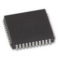
ISPLSI2032E-110LJ44 LATTICE SEMICONDUCTOR, ISPLSI2032E-110LJ44 Datasheet - Page 11

ISPLSI2032E-110LJ44
Manufacturer Part Number
ISPLSI2032E-110LJ44
Description
CMOS ISP EEPLD, SMD, 2032, PLCC44
Manufacturer
LATTICE SEMICONDUCTOR
Datasheet
1.ISPLSI2032E-110LJ44.pdf
(14 pages)
Specifications of ISPLSI2032E-110LJ44
No. Of Macrocells
32
No. Of I/o's
34
Propagation Delay
10ns
Global Clock Setup Time
7.5ns
Frequency
110MHz
Supply Voltage Range
4.75V To 5.25V
Operating Temperature Range
0°C To +70°C
Available stocks
Company
Part Number
Manufacturer
Quantity
Price
Company:
Part Number:
ISPLSI2032E-110LJ44
Manufacturer:
LATTICE
Quantity:
525
Company:
Part Number:
ISPLSI2032E-110LJ44
Manufacturer:
LATTICE
Quantity:
405
Company:
Part Number:
ISPLSI2032E-110LJ44
Manufacturer:
LATTICE
Quantity:
3
Part Number:
ISPLSI2032E-110LJ44
Manufacturer:
LATTICE
Quantity:
20 000
1. Pins have dual function capability.
2. NC pins are not to be connected to any active signals, V
I/O 0 - I/O 3
I/O 4 - I/O 7
I/O 8 - I/O 11
I/O 12 - I/O 15
I/O 16 - I/O 19
I/O 20 - I/O 23
I/O 24 - I/O 27
I/O 28 - I/O 31
GOE 0
Y0
RESET/Y1
BSCAN
TDI/IN 0
TMS/NC
TDO/IN 1
TCK/Y2
GND
VCC
VCCIO
Pin Description
NAME
1
1
2
1
15,
19,
25,
29,
37,
41,
3,
7,
2
11
35
13
14
36
24
33
1,
12, 34
PIN NUMBERS
44-PIN PLCC
23
16,
20,
26,
30,
38,
42,
4,
8,
17,
21,
27,
31,
39,
43,
5,
9,
18,
22,
28,
32,
40,
44,
6,
10
PIN NUMBERS
40
5
29
7
8
18
27
17, 39
6,
30
9,
13,
19,
23,
31
35,
41,
1,
44-PIN TQFP
28
10,
14,
20,
24,
32,
36,
42,
2,
11,
15,
21,
25,
33,
37,
43,
3,
CC
12,
16,
22,
26,
34,
38,
44,
4
or GND.
PIN NUMBERS
9,
14,
20,
25,
33,
38,
44,
1,
5
31
7
8
32
19
29
12, 18, 36, 42
6,
24, 48
43
48-PIN TQFP
11
30
10,
15,
21,
26,
34,
39,
45,
2,
11,
16,
22,
27,
35,
40,
46,
3,
Specifications ispLSI 2032E
13,
17,
23,
28,
37,
41,
47,
4
Global Output Enable input pin.
V
Supply voltage for output drivers, 5V or 3.3V. All
VCCIO pins must be connected to the same voltage
level.
Input/Output Pins — These are the general purpose
I/O pins used by the logic array.
Dedicated Clock input. This clock input is connected to
one of the clock inputs of all the GLBs on the device.
This pin performs two functions:
- Dedicated clock input. This clock input is brought
into the Clock Distribution Network, and can optionally
be routed to any GLB and/or I/O cell on the device.
- Active Low (0) Reset pin which resets all of the GLB
and I/O registers in the device.
Input — Dedicated in-system programming enable
input pin. This pin is brought low to enable the
programming mode. The TMS, TDI, TDO and TCK
controls become active.
Input — When in ISP mode, controls operation of ISP
state machine.
Output/Input — This pin performs two functions. When
BSCAN is logic low, it functions as an output pin to
read serial shift register data. When BSCAN is high, it
functions as a dedicated input pin.
Input — This pin performs two functions. When
BSCAN is logic low, it functions as a clock pin for the
Serial Shift Register. When BSCAN is high, it
functions as a dedicated clock input. This clock input
is brought into the Clock Distribution Network and
can be routed to any GLB and/or I/O cell on the
device.
Ground (GND)
Input — This pin performs two functions. When
BSCAN is logic low, it functions as an input pin to load
programming data into the device. TDI/IN0 also is used
as one of the two control pins for the ISP state
machine. When BSCAN is high, it functions as a
dedicated input pin.
CC
DESCRIPTION
Table 2-0002/2032E


