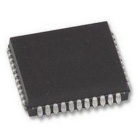
ISPLSI2032E-110LJ44 LATTICE SEMICONDUCTOR, ISPLSI2032E-110LJ44 Datasheet - Page 2

ISPLSI2032E-110LJ44
Manufacturer Part Number
ISPLSI2032E-110LJ44
Description
CMOS ISP EEPLD, SMD, 2032, PLCC44
Manufacturer
LATTICE SEMICONDUCTOR
Datasheet
1.ISPLSI2032E-110LJ44.pdf
(14 pages)
Specifications of ISPLSI2032E-110LJ44
No. Of Macrocells
32
No. Of I/o's
34
Propagation Delay
10ns
Global Clock Setup Time
7.5ns
Frequency
110MHz
Supply Voltage Range
4.75V To 5.25V
Operating Temperature Range
0°C To +70°C
Available stocks
Company
Part Number
Manufacturer
Quantity
Price
Company:
Part Number:
ISPLSI2032E-110LJ44
Manufacturer:
LATTICE
Quantity:
525
Company:
Part Number:
ISPLSI2032E-110LJ44
Manufacturer:
LATTICE
Quantity:
405
Company:
Part Number:
ISPLSI2032E-110LJ44
Manufacturer:
LATTICE
Quantity:
3
Part Number:
ISPLSI2032E-110LJ44
Manufacturer:
LATTICE
Quantity:
20 000
Figure 1. ispLSI 2032E Functional Block Diagram
programmed to be a combinatorial input, output or bi-
directional I/O pin with 3-state control. The signal levels
are TTL compatible voltages and the output drivers can
source 4 mA or sink 8 mA. Each output can be pro-
grammed independently for fast or slow output slew rate
to minimize overall output switching noise. By connecting
the VCCIO pins to a common 5V or 3.3V power supply,
I/O output levels can be matched to 5V or 3.3V compat-
ible voltages. When connected to a 5V supply, the I/O
pins provide PCI-compatible output drive (48-pin device
only).
Eight GLBs, 32 I/O cells, two dedicated inputs and two
ORPs are connected together to make a Megablock (see
Figure 1). The outputs of the eight GLBs are connected
to a set of 32 universal I/O cells by the ORP. Each ispLSI
2032E device contains one Megablock.
The GRP has as its inputs, the outputs from all of the
GLBs and all of the inputs from the bi-directional I/O cells.
All of these signals are made available to the inputs of the
GLBs. Delays through the GRP have been equalized to
minimize timing skew.
Functional Block Diagram
TDO/IN 1
GOE 0
TDI/IN 0
Notes:
BSCAN
I/O 10
I/O 11
I/O 12
I/O 13
I/O 14
I/O 15
*Y1 and RESET are multiplexed on the same pin
I/O 0
I/O 1
I/O 2
I/O 3
I/O 4
I/O 5
I/O 6
I/O 7
I/O 8
I/O 9
TMS
A1
A2
A3
A0
Global Routing Pool
(GRP)
2
Clocks in the ispLSI 2032E device are selected using the
dedicated clock pins. Three dedicated clock pins (Y0, Y1,
Y2) or an asynchronous clock can be selected on a GLB
basis. The asynchronous or Product Term clock can be
generated in any GLB for its own clock.
Programmable Open-Drain Outputs
In addition to the standard output configuration, the
outputs of the ispLSI 2032E are individually program-
mable, either as a standard totem-pole output or an
open-drain output. The totem-pole output drives the
specified Voh and Vol levels, whereas the open-drain
output drives only the specified Vol. The Voh level on the
open-drain output depends on the external loading and
pull-up. This output configuration is controlled by a pro-
grammable fuse. The default configuration when the
device is in bulk erased state is totem-pole configuration.
The open-drain/totem-pole option is selectable through
the Lattice software tools.
Specifications ispLSI 2032E
TCK/Y2
Y1*
Y0
A6
A5
A4
A7
0139/2032E
I/O 31
I/O 30
I/O 29
I/O 28
I/O 27
I/O 26
I/O 25
I/O 24
I/O 23
I/O 22
I/O 21
I/O 20
I/O 19
I/O 18
I/O 17
I/O 16


