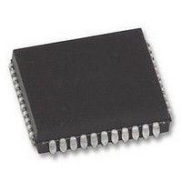
ISPLSI2032E-110LJ44 LATTICE SEMICONDUCTOR, ISPLSI2032E-110LJ44 Datasheet - Page 4

ISPLSI2032E-110LJ44
Manufacturer Part Number
ISPLSI2032E-110LJ44
Description
CMOS ISP EEPLD, SMD, 2032, PLCC44
Manufacturer
LATTICE SEMICONDUCTOR
Datasheet
1.ISPLSI2032E-110LJ44.pdf
(14 pages)
Specifications of ISPLSI2032E-110LJ44
No. Of Macrocells
32
No. Of I/o's
34
Propagation Delay
10ns
Global Clock Setup Time
7.5ns
Frequency
110MHz
Supply Voltage Range
4.75V To 5.25V
Operating Temperature Range
0°C To +70°C
Available stocks
Company
Part Number
Manufacturer
Quantity
Price
Company:
Part Number:
ISPLSI2032E-110LJ44
Manufacturer:
LATTICE
Quantity:
525
Company:
Part Number:
ISPLSI2032E-110LJ44
Manufacturer:
LATTICE
Quantity:
405
Company:
Part Number:
ISPLSI2032E-110LJ44
Manufacturer:
LATTICE
Quantity:
3
Part Number:
ISPLSI2032E-110LJ44
Manufacturer:
LATTICE
Quantity:
20 000
1. One output at a time for a maximum duration of one second (V
2. Meaured using two 16-bit counters.
3. Typical values are at V
4. Unused inputs held at 0.0V.
5. Available in 48-pin package only.
6. Maximum I
Output Load Conditions (see Figure 2)
SYMBOL
V
V
I
I
I
I
I
Input Pulse Levels
Input Rise and Fall Time 10% to 90%
Input Timing Reference Levels
Output Timing Reference Levels
Output Load
3-state levels are measured 0.5V from
steady-state active level.
Switching Test Conditions
DC Electrical Characteristics
IL
IH
IL-PU
OS
CC
OL
OH
Power Consumption section of this data sheet and the Thermal Management section of the Lattice Semiconductor
Data Book or CD-ROM to estimate maximum I
A
B
C
1
2,4,6
TEST CONDITION
Active High
Active Low
Active High to Z
at V -0.5V
Active Low to Z
at V +0.5V
Output Low Voltage
Output High Voltage
Input or I/O Low Leakage Current
Input or I/O High Leakage Current
I/O Active Pull-Up Current, non-PCI
I/O Active Pull-Up Current, PCI
Output Short Circuit Current, non-PCI
Output Short Circuit Current, PCI
Operating Power Supply Current
OH
OL
CC
varies widely with specific device configuration and operating frequency. Refer to the
PARAMETER
CC
= 5V and T
470Ω
470Ω
470Ω
R1
Over Recommended Operating Conditions
∞
∞
A
= 25°C.
5
5
390Ω
390Ω
390Ω
390Ω
390Ω
GND to 3.0V
See Figure 2
R2
Table 2-0003/2032E
CC
1.5 ns
f
I
I
0V ≤ V
(V
V
0V ≤ V
0V ≤ V
V
V
V
1.5V
1.5V
OL
OH
TOGGLE
Table 2 - 0004A
.
CCIO
CCIO
CCIO
IL
CCIO
= 8 mA
= -4 mA
= 0.0V, V
35pF
35pF
35pF
5pF
5pF
CL
≤ V
= 5.0V or 3.3V, V
= 5V, V
- 0.2)V ≤ V
IN
IN
IN
= 1 MHz
≤ 2.0V
≤ V
IN
≤ 2.0V
≤ 5.25V
IL
4
IH
OUT
OUT
Figure 2. Test Load
(Max.)
CONDITION
= 3.0V
IN
= 0.5V
= 0.5V). Characterized, but not 100% tested.
*
Device
Output
Specifications ispLSI 2032E
C L includes Test Fixture and Probe Capacitance.
≤ V
CCIO
OUT
= 0.5V
-225/-200
Others
1
+ 5V
MIN.
R 1
R 2
2.4
-10
-10
–
–
–
–
–
–
–
–
TYP.
85
65
C L
–
–
–
–
–
–
–
–
–
*
3
MAX. UNITS
-150
-250
-200
-240
0.4
-10
10
10
Table 2-0007/2032E
–
–
–
Point
Test
0213A
mA
mA
mA
mA
µA
µA
µA
µA
µA
V
V


