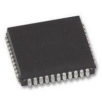
ISPLSI2032E-110LJ44 LATTICE SEMICONDUCTOR, ISPLSI2032E-110LJ44 Datasheet - Page 6

ISPLSI2032E-110LJ44
Manufacturer Part Number
ISPLSI2032E-110LJ44
Description
CMOS ISP EEPLD, SMD, 2032, PLCC44
Manufacturer
LATTICE SEMICONDUCTOR
Datasheet
1.ISPLSI2032E-110LJ44.pdf
(14 pages)
Specifications of ISPLSI2032E-110LJ44
No. Of Macrocells
32
No. Of I/o's
34
Propagation Delay
10ns
Global Clock Setup Time
7.5ns
Frequency
110MHz
Supply Voltage Range
4.75V To 5.25V
Operating Temperature Range
0°C To +70°C
Available stocks
Company
Part Number
Manufacturer
Quantity
Price
Company:
Part Number:
ISPLSI2032E-110LJ44
Manufacturer:
LATTICE
Quantity:
525
Company:
Part Number:
ISPLSI2032E-110LJ44
Manufacturer:
LATTICE
Quantity:
405
Company:
Part Number:
ISPLSI2032E-110LJ44
Manufacturer:
LATTICE
Quantity:
3
Part Number:
ISPLSI2032E-110LJ44
Manufacturer:
LATTICE
Quantity:
20 000
1. Unless noted otherwise, all parameters use a GRP load of four GLBs, 20 PTXOR path, ORP and Y0 clock.
2. Refer to Timing Model in this data sheet for further details.
3. Standard 16-bit counter using GRP feedback.
4. Reference Switching Test Conditions section.
t
t
f
f
f
t
t
t
t
t
t
t
t
t
t
t
t
t
t
External Timing Parameters
PARAMETER
pd1
pd2
max
max (Ext.)
max (Tog.)
su1
co1
h1
su2
co2
h2
r1
rw1
ptoeen
ptoedis
goeen
goedis
wh
wl
COND.
TEST
A
A
A
A
A
B
C
B
C
–
–
–
–
–
–
–
–
–
–
4
10 GLB Register Clock to Output Delay
11 GLB Register Hold Time after Clock
12 External Reset Pin to Output Delay, ORP Bypass
13 External Reset Pulse Duration
14 Input to Output Enable
15 Input to Output Disable
16 Global OE Output Enable
17 Global OE Output Disable
18 External Synchronous Clock Pulse Duration, High
19 External Synchronous Clock Pulse Duration, Low
#
1 Data Propagation Delay, 4PT Bypass, ORP Bypass
2 Data Propagation Delay
3 Clock Frequency with Internal Feedback
4 Clock Frequency with External Feedback
5 Clock Frequency, Max. Toggle
6 GLB Register Setup Time before Clock, 4 PT Bypass
7 GLB Register Clock to Output Delay, ORP Bypass
8 GLB Register Hold Time after Clock, 4 PT Bypass
9 GLB Register Setup Time before Clock
2
Over Recommended Operating Conditions
DESCRIPTION
6
1
Specifications ispLSI 2032E
3
(
tsu2 + tco1
1
)
MIN.
100
167
137
4.0
0.0
5.5
0.0
5.0
3.0
3.0
–
–
–
–
–
–
–
–
–
-135
MAX.
10.0
12.0
12.0
7.5
4.5
5.5
9.0
6.0
6.0
–
–
–
–
–
–
–
–
–
–
MIN.
77.0
111
125
5.5
0.0
7.5
0.0
6.5
4.0
4.0
–
–
–
–
–
–
–
–
–
-110
MAX.
Table 2-0030B/2032E
10.0
13.0
12.5
14.5
14.5
5.5
6.5
7.0
7.0
–
–
–
–
–
–
–
–
–
–
UNITS
MHz
MHz
MHz
ns
ns
ns
ns
ns
ns
ns
ns
ns
ns
ns
ns
ns
ns
ns
ns


