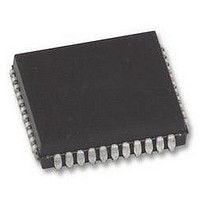
ISPLSI2032E-110LJ44 LATTICE SEMICONDUCTOR, ISPLSI2032E-110LJ44 Datasheet - Page 7

ISPLSI2032E-110LJ44
Manufacturer Part Number
ISPLSI2032E-110LJ44
Description
CMOS ISP EEPLD, SMD, 2032, PLCC44
Manufacturer
LATTICE SEMICONDUCTOR
Datasheet
1.ISPLSI2032E-110LJ44.pdf
(14 pages)
Specifications of ISPLSI2032E-110LJ44
No. Of Macrocells
32
No. Of I/o's
34
Propagation Delay
10ns
Global Clock Setup Time
7.5ns
Frequency
110MHz
Supply Voltage Range
4.75V To 5.25V
Operating Temperature Range
0°C To +70°C
Available stocks
Company
Part Number
Manufacturer
Quantity
Price
Company:
Part Number:
ISPLSI2032E-110LJ44
Manufacturer:
LATTICE
Quantity:
525
Company:
Part Number:
ISPLSI2032E-110LJ44
Manufacturer:
LATTICE
Quantity:
405
Company:
Part Number:
ISPLSI2032E-110LJ44
Manufacturer:
LATTICE
Quantity:
3
Part Number:
ISPLSI2032E-110LJ44
Manufacturer:
LATTICE
Quantity:
20 000
1. Internal Timing Parameters are not tested and are for reference only.
2. Refer to Timing Model in this data sheet for further details.
3. The XOR adjacent path can only be used by hard macros.
Internal Timing Parameters
PARAMETER
Inputs
t
t
GRP
t
GLB
t
t
t
t
t
t
t
t
t
t
t
t
t
ORP
t
t
Outputs
t
t
t
t
t
Clocks
t
t
Global Reset
t
io
din
grp
4ptbpc
4ptbpr
1ptxor
20ptxor
xoradj
gbp
gsu
gh
gco
gro
ptre
ptoe
ptck
orp
orpbp
ob
sl
oen
odis
goe
gy0
gy1/2
gr
20 Input Buffer Delay
21 Dedicated Input Delay
22 GRP Delay
23 4 Product Term Bypass Path Delay (Combinatorial)
24 4 Product Term Bypass Path Delay (Registered)
25 1 Product Term/XOR Path Delay
26 20 Product Term/XOR Path Delay
27 XOR Adjacent Path Delay
28 GLB Register Bypass Delay
29 GLB Register Setup Time before Clock
30 GLB Register Hold Time after Clock
31 GLB Register Clock to Output Delay
32 GLB Register Reset to Output Delay
33 GLB Product Term Reset to Register Delay
34 GLB Product Term Output Enable to I/O Cell Delay
35 GLB Product Term Clock Delay
36 ORP Delay
37 ORP Bypass Delay
38 Output Buffer Delay
39 Output Slew Limited Delay Adder
40 I/O Cell OE to Output Enabled
41 I/O Cell OE to Output Disabled
42 Global Output Enable
43 Clock Delay, Y0 to Global GLB Clock Line (Ref. clock)
44 Clock Delay, Y1 or Y2 to Global GLB Clock Line
45 Global Reset to GLB
#
2
Over Recommended Operating Conditions
1
DESCRIPTION
3
7
Specifications ispLSI 2032E
MIN. MAX.
0.8
1.7
0.3
0.8
1.0
–
–
–
–
–
–
–
–
–
–
–
–
–
–
–
–
–
–
–
–
–
-225
1.0
0.0
1.0
1.5
1.5
1.5
2.0
0.8
1.0
2.7
0.6
1.3
0.7
1.2
1.2
2.2
2.2
2.2
0.0
0.7
1.3
2.5
4.2
2.8
–
–
MIN.
0.8
1.7
0.7
1.2
1.4
–
–
–
–
–
–
–
–
–
–
–
–
–
–
–
–
–
–
–
–
–
-200
MAX.
1.0
0.0
0.6
1.5
1.5
1.5
2.0
1.2
1.4
2.7
0.4
1.3
1.8
1.8
2.8
2.8
2.8
0.0
0.7
2.9
2.5
4.4
0.7
3.2
–
–
MIN.
0.3
2.7
1.5
1.4
1.6
–
–
–
–
–
–
–
–
–
–
–
–
–
–
–
–
–
–
–
–
–
-180
MAX.
Table 2-0036A/2032E
0.6
1.3
0.7
1.8
2.8
3.8
3.8
3.8
0.0
0.7
1.1
2.9
5.9
3.7
1.1
0.6
1.3
1.5
2.8
2.8
2.2
1.4
1.6
3.5
–
–
UNITS
ns
ns
ns
ns
ns
ns
ns
ns
ns
ns
ns
ns
ns
ns
ns
ns
ns
ns
ns
ns
ns
ns
ns
ns
ns
ns


