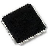
LPC2378FBD144 NXP Semiconductors, LPC2378FBD144 Datasheet - Page 21

LPC2378FBD144
Manufacturer Part Number
LPC2378FBD144
Description
MCU 32BIT ARM7, 10/100, USB, CAN
Manufacturer
NXP Semiconductors
Datasheet
1.LPC2378FBD144.pdf
(68 pages)
Specifications of LPC2378FBD144
Core Size
32bit
No. Of I/o's
104
Program Memory Size
512KB
Ram Memory Size
58KB
Cpu Speed
72MHz
Oscillator Type
External, Internal
No. Of Timers
4
No. Of Pwm Channels
6
Digital Ic Case
RoHS Compliant
Controller Family/series
LPC23xx
Rohs Compliant
Yes
Available stocks
Company
Part Number
Manufacturer
Quantity
Price
Company:
Part Number:
LPC2378FBD144
Manufacturer:
ST
Quantity:
43
Company:
Part Number:
LPC2378FBD144
Manufacturer:
NXP
Quantity:
5 000
Company:
Part Number:
LPC2378FBD144,551
Manufacturer:
ADI
Quantity:
2 397
Company:
Part Number:
LPC2378FBD144,551
Manufacturer:
NXP Semiconductors
Quantity:
10 000
NXP Semiconductors
LPC2377_78
Product data sheet
7.9.1 Features
7.9 Fast general purpose parallel I/O
Device pins that are not connected to a specific peripheral function are controlled by the
GPIO registers. Pins may be dynamically configured as inputs or outputs. Separate
registers allow setting or clearing any number of outputs simultaneously. The value of the
output register may be read back as well as the current state of the port pins.
The LPC2377/78 use accelerated GPIO functions:
Additionally, any pin on Port 0 and Port 2 (total of 46 pins) providing a digital function can
be programmed to generate an interrupt on a rising edge, a falling edge, or both. The
edge detection is asynchronous, so it may operate when clocks are not present such as
during Power-down mode. Each enabled interrupt can be used to wake up the chip from
Power-down mode.
•
•
•
•
•
•
•
•
•
•
•
•
•
•
•
•
32-bit AHB master bus width.
Incrementing or non-incrementing addressing for source and destination.
Programmable DMA burst size. The DMA burst size can be programmed to more
efficiently transfer data. Usually the burst size is set to half the size of the FIFO in the
peripheral.
Internal four-word FIFO per channel.
Supports 8-bit, 16-bit, and 32-bit wide transactions.
An interrupt to the processor can be generated on a DMA completion or when a DMA
error has occurred.
Interrupt masking. The DMA error and DMA terminal count interrupt requests can be
masked.
Raw interrupt status. The DMA error and DMA count raw interrupt status can be read
prior to masking.
GPIO registers are relocated to the ARM local bus so that the fastest possible I/O
timing can be achieved.
Mask registers allow treating sets of port bits as a group, leaving other bits
unchanged.
All GPIO registers are byte and half-word addressable.
Entire port value can be written in one instruction.
Bit level set and clear registers allow a single instruction to set or clear any number of
bits in one port.
Direction control of individual bits.
All I/O default to inputs after reset.
Backward compatibility with other earlier devices is maintained with legacy Port 0 and
Port 1 registers appearing at the original addresses on the APB bus.
All information provided in this document is subject to legal disclaimers.
Rev. 5 — 17 June 2010
Single-chip 16-bit/32-bit microcontrollers
LPC2377/78
© NXP B.V. 2010. All rights reserved.
21 of 68


