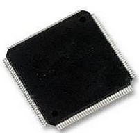
LPC2378FBD144 NXP Semiconductors, LPC2378FBD144 Datasheet - Page 36

LPC2378FBD144
Manufacturer Part Number
LPC2378FBD144
Description
MCU 32BIT ARM7, 10/100, USB, CAN
Manufacturer
NXP Semiconductors
Datasheet
1.LPC2378FBD144.pdf
(68 pages)
Specifications of LPC2378FBD144
Core Size
32bit
No. Of I/o's
104
Program Memory Size
512KB
Ram Memory Size
58KB
Cpu Speed
72MHz
Oscillator Type
External, Internal
No. Of Timers
4
No. Of Pwm Channels
6
Digital Ic Case
RoHS Compliant
Controller Family/series
LPC23xx
Rohs Compliant
Yes
Available stocks
Company
Part Number
Manufacturer
Quantity
Price
Company:
Part Number:
LPC2378FBD144
Manufacturer:
ST
Quantity:
43
Company:
Part Number:
LPC2378FBD144
Manufacturer:
NXP
Quantity:
5 000
Company:
Part Number:
LPC2378FBD144,551
Manufacturer:
ADI
Quantity:
2 397
Company:
Part Number:
LPC2378FBD144,551
Manufacturer:
NXP Semiconductors
Quantity:
10 000
NXP Semiconductors
LPC2377_78
Product data sheet
CAUTION
7.26.4 AHB
7.26.5 External interrupt inputs
7.26.6 Memory mapping control
7.27 Emulation and debugging
Running an application with level CRP3 selected fully disables any access to chip via the
JTAG pins and the ISP. This mode effectively disables ISP override using P2[10] pin, too.
It is up to the user’s application to provide (if needed) flash update mechanism using IAP
calls or call reinvoke ISP command to enable flash update via UART0.
The LPC2377/78 implement two AHBs in order to allow the Ethernet block to operate
without interference caused by other system activity. The primary AHB, referred to as
AHB1, includes the Vectored Interrupt Controller, GPDMA controller, USB interface, and
8 kB SRAM primarily intended for use by the USB.
The second AHB, referred to as AHB2, includes only the Ethernet block and an
associated 16 kB SRAM. In addition, a bus bridge is provided that allows the secondary
AHB to be a bus master on AHB1, allowing expansion of Ethernet buffer space into
off-chip memory or unused space in memory residing on AHB1.
In summary, bus masters with access to AHB1 are the ARM7 itself, the USB block, the
GPDMA function, and the Ethernet block (via the bus bridge from AHB2). Bus masters
with access to AHB2 are the ARM7 and the Ethernet block.
The LPC2377/78 include up to 50 edge sensitive interrupt inputs combined with up to four
level sensitive external interrupt inputs as selectable pin functions. The external interrupt
inputs can optionally be used to wake up the processor from Power-down mode.
The memory mapping control alters the mapping of the interrupt vectors that appear at the
beginning at address 0x0000 0000. Vectors may be mapped to the bottom of the Boot
ROM, the SRAM, or external memory. This allows code running in different memory
spaces to have control of the interrupts.
The LPC2377/78 support emulation and debugging via a JTAG serial port. A trace port
allows tracing program execution. Debugging and trace functions are multiplexed only
with GPIOs on P2[0] to P2[9]. This means that all communication, timer, and interface
peripherals residing on other pins are available during the development and debugging
phase as they are when the application is run in the embedded system itself.
If level three Code Read Protection (CRP3) is selected, no future factory testing can be
performed on the device.
All information provided in this document is subject to legal disclaimers.
Rev. 5 — 17 June 2010
Single-chip 16-bit/32-bit microcontrollers
LPC2377/78
© NXP B.V. 2010. All rights reserved.
36 of 68


