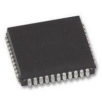
P89V51RB2FA NXP Semiconductors, P89V51RB2FA Datasheet - Page 14

P89V51RB2FA
Manufacturer Part Number
P89V51RB2FA
Description
MCU 8BIT 80C51 16K FLASH, PLCC44
Manufacturer
NXP Semiconductors
Datasheet
1.P89V51RC2FBC557.pdf
(80 pages)
Specifications of P89V51RB2FA
Controller Family/series
(8051) 8052
Core Size
8bit
No. Of I/o's
32
Program Memory Size
16KB
Ram Memory Size
1KB
Cpu Speed
40MHz
Oscillator Type
External Only
No. Of Timers
4
No. Of Pwm
RoHS Compliant
Available stocks
Company
Part Number
Manufacturer
Quantity
Price
Company:
Part Number:
P89V51RB2FA
Manufacturer:
NXP
Quantity:
1 000
Company:
Part Number:
P89V51RB2FA
Manufacturer:
NXP
Quantity:
2 000
Part Number:
P89V51RB2FA
Manufacturer:
NXP/恩智浦
Quantity:
20 000
Part Number:
P89V51RB2FA (FLA
Manufacturer:
NXP/恩智浦
Quantity:
20 000
Company:
Part Number:
P89V51RB2FA,529
Manufacturer:
NXP Semiconductors
Quantity:
10 000
Company:
Part Number:
P89V51RB2FAЈ¬529
Manufacturer:
NXP
Quantity:
150
NXP Semiconductors
P89V51RB2_RC2_RD2_5
Product data sheet
6.2.1 Flash program memory bank selection
6.2.2 Power-on reset code execution
6.2 Memory organization
The device has separate address spaces for program and data memory.
There are two internal flash memory blocks in the device. Block 0 has 16/32/64 kB and is
organized as 128/256/512 sectors, each sector consists of 128 B. Block 1 contains the
IAP/ISP routines and may be enabled such that it overlays the first 8 kB of the user code
memory. The overlay function is controlled by the combination of the Software Reset Bit
(SWR) at FCF.1 and the Bank Select Bit (BSEL) at FCF.0. The combination of these bits
and the memory source used for instructions is shown in
Table 5.
Access to the IAP routines in block 1 may be enabled by clearing the BSEL bit (FCF.0),
provided that the SWR bit (FCF.1) is cleared. Following a power-on sequence, the boot
code is automatically executed and attempts to autobaud to a host. If no autobaud occurs
within approximately 400 ms and the SoftICE flag is not set, control will be passed to the
user code. A software reset is used to accomplish this control transfer and as a result the
SWR bit will remain set. Therefore the user's code will need to clear the SWR bit in
order to access the IAP routines in block 1. However, caution must be taken when
dynamically changing the BSEL bit. Since this will cause different physical memory to be
mapped to the logical program address space, the user must avoid clearing the BSEL bit
when executing user code within the address range 0000H to 1FFFH.
At initial power up, the port pins will be in a random state until the oscillator has started
and the internal reset algorithm has weakly pulled all pins high. Powering up the device
without a valid reset could cause the MCU to start executing instructions from an
indeterminate location. Such undefined states may inadvertently corrupt the code in the
flash. A system reset will not affect the 1 kB of on-chip RAM while the device is running,
however, the contents of the on-chip RAM during power up are indeterminate.
When power is applied to the device, the RST pin must be held high long enough for the
oscillator to start up (usually several milliseconds for a low frequency crystal), in addition
to two machine cycles for a valid power-on reset. An example of a method to extend the
RST signal is to implement a RC circuit by connecting the RST pin to V
capacitor and to V
circuit is being used, provisions should be made to ensure the V
exceed 1 ms and the oscillator start-up time does not exceed 10 ms.
For a low frequency oscillator with slow start-up time the reset signal must be extended in
order to account for the slow start-up time. This method maintains the necessary
relationship between V
which may cause corruption in the code of the flash. The power-on detection is designed
SWR (FCF.1)
0
0
1
1
Code memory bank selection
SS
BSEL (FCF.0)
0
1
0
1
Rev. 05 — 12 November 2009
through an 8.2 k resistor as shown in
DD
and RST to avoid programming at an indeterminate location,
Addresses from 0000H to
1FFFH
boot code (in block 1)
user code (in block 0)
P89V51RB2/RC2/RD2
8-bit microcontrollers with 80C51 core
Table
Figure
5.
Addresses above 1FFFH
user code (in block 0)
DD
rise time does not
5. Note that if an RC
DD
© NXP B.V. 2009. All rights reserved.
through a 10 F
14 of 80


