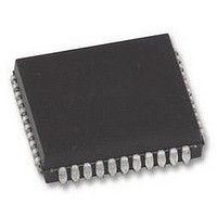
P89V51RB2FA NXP Semiconductors, P89V51RB2FA Datasheet - Page 7

P89V51RB2FA
Manufacturer Part Number
P89V51RB2FA
Description
MCU 8BIT 80C51 16K FLASH, PLCC44
Manufacturer
NXP Semiconductors
Datasheet
1.P89V51RC2FBC557.pdf
(80 pages)
Specifications of P89V51RB2FA
Controller Family/series
(8051) 8052
Core Size
8bit
No. Of I/o's
32
Program Memory Size
16KB
Ram Memory Size
1KB
Cpu Speed
40MHz
Oscillator Type
External Only
No. Of Timers
4
No. Of Pwm
RoHS Compliant
Available stocks
Company
Part Number
Manufacturer
Quantity
Price
Company:
Part Number:
P89V51RB2FA
Manufacturer:
NXP
Quantity:
1 000
Company:
Part Number:
P89V51RB2FA
Manufacturer:
NXP
Quantity:
2 000
Part Number:
P89V51RB2FA
Manufacturer:
NXP/恩智浦
Quantity:
20 000
Part Number:
P89V51RB2FA (FLA
Manufacturer:
NXP/恩智浦
Quantity:
20 000
Company:
Part Number:
P89V51RB2FA,529
Manufacturer:
NXP Semiconductors
Quantity:
10 000
Company:
Part Number:
P89V51RB2FAЈ¬529
Manufacturer:
NXP
Quantity:
150
NXP Semiconductors
Table 3.
P89V51RB2_RC2_RD2_5
Product data sheet
Symbol
P1.2/ECI
P1.3/CEX0
P1.4/SS/CEX1 5
P1.5/MOSI/
CEX2
P1.6/MISO/
CEX3
P1.7/SPICLK/
CEX4
P2.0 to P2.7
P2.0/A8
P2.1/A9
P2.2/A10
P2.3/A11
P2.4/A12
P89V51RB2/RC2/RD2 pin description
Pin
DIP40
3
4
6
7
8
21
22
23
24
25
TQFP44
42
43
44
1
2
3
18
19
20
21
22
PLCC44
4
5
6
7
8
9
24
25
26
27
28
Rev. 05 — 12 November 2009
…continued
Type
I/O
I
I/O
I/O
I/O
I
I/O
I/O
I/O
I/O
I/O
I/O
I/O
I/O
I/O
I/O
I/O with
internal
pull-up
I/O
O
I/O
O
I/O
O
I/O
O
I/O
O
Description
P1.2 — Port 1 bit 2.
ECI — External clock input. This signal is the external
clock input for the PCA.
P1.3 — Port 1 bit 3.
CEX0 — Capture/compare external I/O for PCA Module 0.
Each capture/compare module connects to a Port 1 pin for
external I/O. When not used by the PCA, this pin can
handle standard I/O.
P1.4 — Port 1 bit 4.
SS — Slave port select input for SPI.
CEX1 — Capture/compare external I/O for PCA Module 1.
P1.5 — Port 1 bit 5.
MOSI — Master Output Slave Input for SPI.
CEX2 — Capture/compare external I/O for PCA Module 2.
P1.6 — Port 1 bit 6.
MISO — Master Input Slave Output for SPI.
CEX3 — Capture/compare external I/O for PCA Module 3.
P1.7 — Port 1 bit 7.
SPICLK — Serial clock input/output for SPI.
CEX4 — Capture/compare external I/O for PCA Module 4.
Port 2: Port 2 is an 8-bit bidirectional I/O port with internal
pull-ups. Port 2 pins are pulled HIGH by the internal
pull-ups when ‘1’s are written to them and can be used as
inputs in this state. As inputs, Port 2 pins that are
externally pulled LOW will source current (I
the internal pull-ups. Port 2 sends the high-order address
byte during fetches from external program memory and
during accesses to external Data Memory that use 16-bit
address (MOVX@DPTR). In this application, it uses strong
internal pull-ups when transitioning to ‘1’s. Port 2 also
receives some control signals and a partial of high-order
address bits during the external host mode programming
and verification.
P2.0 — Port 2 bit 0.
A8 — Address bit 8.
P2.1 — Port 2 bit 1.
A9 — Address bit 9.
P2.2 — Port 2 bit 2.
A10 — Address bit 10.
P2.3 — Port 2 bit 3.
A11 — Address bit 11.
P2.4 — Port 2 bit 4.
A12 — Address bit 12.
P89V51RB2/RC2/RD2
8-bit microcontrollers with 80C51 core
© NXP B.V. 2009. All rights reserved.
IL
) because of
7 of 80


