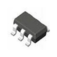
DAC121S101CIMK National Semiconductor, DAC121S101CIMK Datasheet - Page 15

DAC121S101CIMK
Manufacturer Part Number
DAC121S101CIMK
Description
IC,D/A CONVERTER,SINGLE,12-BIT,CMOS,TSSOP,8PIN
Manufacturer
National Semiconductor
Datasheet
1.DAC121S101CIMK.pdf
(20 pages)
Specifications of DAC121S101CIMK
Rohs Compliant
NO
Number Of Channels
1
Resolution
12b
Interface Type
Serial (3-Wire, SPI, QSPI, Microwire)
Single Supply Voltage (typ)
3.3/5V
Dual Supply Voltage (typ)
Not RequiredV
Settling Time
10us
Architecture
Resistor-String
Power Supply Requirement
Single
Output Type
Voltage
Integral Nonlinearity Error
±8LSB
Single Supply Voltage (min)
2.7V
Single Supply Voltage (max)
5.5V
Dual Supply Voltage (min)
Not RequiredV
Dual Supply Voltage (max)
Not RequiredV
Operating Temp Range
-40C to 105C
Operating Temperature Classification
Industrial
Mounting
Surface Mount
Pin Count
6
Package Type
TSOT
Lead Free Status / Rohs Status
Not Compliant
Available stocks
Company
Part Number
Manufacturer
Quantity
Price
Part Number:
DAC121S101CIMK
Manufacturer:
NS/国半
Quantity:
20 000
Company:
Part Number:
DAC121S101CIMK/NOPB
Manufacturer:
MICROCHIP
Quantity:
1 001
Part Number:
DAC121S101CIMK/NOPB
Manufacturer:
TI/德州仪器
Quantity:
20 000
Part Number:
DAC121S101CIMKX
Manufacturer:
TI/德州仪器
Quantity:
20 000
Company:
Part Number:
DAC121S101CIMKX/NOPB
Manufacturer:
TI
Quantity:
15 000
1.6 POWER-ON RESET
The power-on reset circuit controls the output voltage during
power-up. Upon application of power the DAC register is filled
with zeros and the output voltage is 0 Volts and remains there
until a valid write sequence is made to the DAC.
1.7 POWER-DOWN MODES
The DAC121S101 has four modes of operation. These
modes are set with two bits (DB13 and DB12) in the control
register.
When both DB13 and DB12 are 0, the device operates nor-
mally. For the other three possible combinations of these bits
the supply current drops to its power-down level and the out-
put is pulled down with either a 1kΩ or a 100KΩ resistor, or
is in a high impedance state, as described in
The bias generator, output amplifier, the resistor string and
other linear circuitry are all shut down in any of the power-
down modes. However, the contents of the DAC register are
unaffected when in power-down, so when coming out of pow-
er down the output voltage returns to the same voltage it was
before entering power down. Minimum power consumption is
achieved in the power-down mode with SCLK disabled and
SYNC and D
Up Time) is typically t
Characteristics Table.
2.0 Applications Information
The simplicity of the DAC121S101 implies ease of use. How-
ever, it is important to recognize that any data converter that
utilizes its supply voltage as its reference voltage will have
essentially zero PSRR (Power Supply Rejection Ratio).
Therefore, it is necessary to provide a noise-free supply volt-
age to the device.
2.1 DSP/MICROPROCESSOR INTERFACING
Interfacing the DAC121S101 to microprocessors and DSPs
is quite simple. The following guidelines are offered to hasten
the design process.
2.1.1 ADSP-2101/ADSP2103 Interfacing
Figure 5
and the ADSP-2101/ADSP2103. The DSP should be set to
operate in the SPORT Transmit Alternate Framing Mode. It is
programmed through the SPORT control register and should
be configured for Internal Clock Operation, Active Low Fram-
ing and 16-bit Word Length. Transmission is started by writing
a word to the Tx register after the SPORT mode has been
enabled.
DB13
0
0
1
1
shows a serial interface between the DAC121S101
IN
DB12
TABLE 1. Modes of Operation
idled low. The time to exit power-down (Wake-
0
1
0
1
WU
Operating Mode
Normal Operation
Power-Down with 1kΩ to GND
Power-Down with 100kΩ to GND
Power-Down with Hi-Z
µsec as stated in the A.C. and Timing
Table
1.
15
2.1.2 80C51/80L51 Interface
A serial interface between the DAC121S101 and the
80C51/80L51 microcontroller is shown in
SYNC signal comes from a bit-programmable pin on the mi-
crocontroller. The example shown here uses port line P3.3.
This line is taken low when data is to transmitted to the
DAC121S101. Since the 80C51/80L51 transmits 8-bit bytes,
only eight falling clock edges occur in the transmit cycle. To
load data into the DAC, the P3.3 line must be left low after the
first eight bits are transmitted. A second write cycle is initiated
to transmit the second byte of data, after which port line P3.3
is brought high. The 80C51/80L51 transmit routine must rec-
ognize that the 80C51/80L51 transmits data with the LSB first
while the DAC121S101 requires data with the MSB first.
2.1.3 68HC11 Interface
A serial interface between the DAC121S101 and the 68HC11
microcontroller is shown in
DAC121S101 is driven from a port line (PC7 in the figure),
similar to the 80C51/80L51.
The 68HC11 should be configured with its CPOL bit as a zero
and its CPHA bit as a one. This configuration causes data on
the MOSI output to be valid on the falling edge of SCLK. PC7
is taken low to transmit data to the DAC. The 68HC11 trans-
mits data in 8-bit bytes with eight falling clock edges. Data is
transmitted with the MSB first. PC7 must remain low after the
first eight bits are transferred. A second write cycle is initiated
to transmit the second byte of data to the DAC, after which
PC7 should be raised to end the write sequence.
FIGURE 5. ADSP-2101/2103 Interface
FIGURE 6. 80C51/80L51 Interface
FIGURE 7. 68HC11 Interface
Figure
7. The SYNC line of the
Figure
www.national.com
20114909
6. The
20114910
20114911


