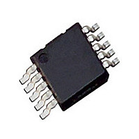
DAC124S085CIMM National Semiconductor, DAC124S085CIMM Datasheet - Page 4

DAC124S085CIMM
Manufacturer Part Number
DAC124S085CIMM
Description
IC,D/A CONVERTER,QUAD,12-BIT,CMOS,TSSOP,10PIN
Manufacturer
National Semiconductor
Datasheet
1.DAC124S085CIMM.pdf
(20 pages)
Specifications of DAC124S085CIMM
Rohs Compliant
NO
Number Of Channels
4
Resolution
12b
Interface Type
SER 3W SPI QSPI UW
Single Supply Voltage (typ)
3.3/5V
Dual Supply Voltage (typ)
Not RequiredV
Settling Time
8.5us
Architecture
Resistor-String
Power Supply Requirement
Single
Output Type
Voltage
Single Supply Voltage (min)
2.7V
Single Supply Voltage (max)
5.5V
Dual Supply Voltage (min)
Not RequiredV
Dual Supply Voltage (max)
Not RequiredV
Operating Temp Range
-40C to 105C
Operating Temperature Classification
Industrial
Mounting
Surface Mount
Pin Count
10
Lead Free Status / Rohs Status
Not Compliant
Available stocks
Company
Part Number
Manufacturer
Quantity
Price
Part Number:
DAC124S085CIMM
Manufacturer:
NS/国半
Quantity:
20 000
Company:
Part Number:
DAC124S085CIMM/NOPB
Manufacturer:
ADI
Quantity:
9 712
Company:
Part Number:
DAC124S085CIMMX
Manufacturer:
TI
Quantity:
6 000
Part Number:
DAC124S085CIMMX
Manufacturer:
NS/国半
Quantity:
20 000
www.national.com
STATIC PERFORMANCE
OUTPUT CHARACTERISTICS
Symbol
Absolute Maximum Ratings
If Military/Aerospace specified devices are required,
please contact the National Semiconductor Sales Office/
Distributors for availability and specifications.
Electrical Characteristics
The following specifications apply for V
48 to 4047. Boldface limits apply for T
TC GE
ZCED
Supply Voltage, V
Voltage on any Input Pin
Input Current at Any Pin (Note 3)
Package Input Current (Note 3)
Power Consumption at T
ESD Susceptibility (Note 5)
Human Body Model
Machine Model
Junction Temperature
Storage Temperature
DNL
ZCO
FSO
FSE
INL
GE
I
ZE
I
OS
OZ
Resolution
Monotonicity
Integral Non-Linearity
Differential Non-Linearity
Zero Code Error
Full-Scale Error
Gain Error
Zero Code Error Drift
Gain Error Tempco
Output Voltage Range
High-Impedance Output
Leakage Current (Note 10)
Zero Code Output
Full Scale Output
Output Short Circuit Current
(source)
A
Parameter
A
= 25°C
A
MIN
= +2.7V to +5.5V, V
−65°C to +150°C
≤
−0.3V to 6.5V
T
See (Note 4)
A
(Notes 1, 2)
V
V
I
I
All ones Loaded to DAC register
V
V
(Note 10)
V
V
V
V
V
V
V
V
V
Input Code = FFFh
V
Input Code = FFFh
OUT
OUT
≤
A
A
A
A
A
A
A
A
A
A
A
A
A
A
= 2.7V to 5.5V
= 4.5V to 5.5V (Note 10)
= 3V
= 5V
= 3V, I
= 3V, I
= 5V, I
= 5V, I
= 3V, I
= 3V, I
= 5V, I
= 5V, I
= 3V, V
= 5V, V
T
+150°C
= 0
= 0
10 mA
20 mA
2500V
MAX
250V
6.5V
and all other limits are at T
OUT
OUT
OUT
OUT
OUT
OUT
OUT
OUT
OUT
OUT
REFIN
= 200 µA
= 1 mA
= 200 µA
= 1 mA
= 200 µA
= 1 mA
= 200 µA
= 1 mA
Conditions
= 0V,
= 0V,
4
= V
Operating Ratings
Package Thermal Resistances
Soldering
Semiconductor's Reflow Temperature Profile specifications.
Refer to www.national.com/packaging. (Note 6)
Operating Temperature Range
Supply Voltage, V
Reference Voltage, V
Digital Input Voltage (Note 7)
Output Load
SCLK Frequency
A
, C
L
= 200 pF to GND, f
10-Lead MSOP
10-Lead LLP
Package
process
A
= 25°C, unless otherwise specified.
A
REFIN
(Note 9)
Typical
±0.15
must
2.984
2.934
4.989
4.958
±2.4
+0.2
−0.1
−0.1
−0.2
−0.7
−1.0
10.0
−20
SCLK
-56
-69
1.3
6.0
7.0
+4
= 30 MHz, input code range
(Notes 1, 2)
comply
(Note 9)
−40°C
Limits
V
−0.75
+0.7
−0.5
±0.5
−1.0
+15
REFIN
12
12
±8
±1
240°C/W
250°C/W
0
θ
≤
JA
with
+2.7V to 5.5V
Up to 40 MHz
T
0 to 1500 pF
0.0V to 5.5V
+1.0V to V
A
%FSR (max)
≤
LSB (max)
LSB (max)
LSB (max)
LSB (min)
mV (max)
Bits (min)
Bits (min)
µA (max)
(Limits)
V (max)
ppm/°C
ppm/°C
V (min)
+105°C
National
%FSR
µV/°C
Units
mV
mV
mV
mV
mA
mA
V
V
V
V
A


