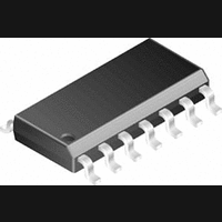
LMC6464AIM National Semiconductor, LMC6464AIM Datasheet - Page 11

LMC6464AIM
Manufacturer Part Number
LMC6464AIM
Description
Operational Amplifier (Op-Amp) IC
Manufacturer
National Semiconductor
Specifications of LMC6464AIM
No. Of Amplifiers
4
Slew Rate
0.015V/µs
No. Of Pins
14
Operating Temperature Range
-40°C To +85°C
Peak Reflow Compatible (260 C)
No
Leaded Process Compatible
No
Mounting Type
Surface Mount
Lead Free Status / RoHS Status
Contains lead / RoHS non-compliant
Available stocks
Company
Part Number
Manufacturer
Quantity
Price
Part Number:
LMC6464AIM
Manufacturer:
NS/国半
Quantity:
20 000
Company:
Part Number:
LMC6464AIMX
Manufacturer:
Texas Instruments
Quantity:
5
Part Number:
LMC6464AIMX
Manufacturer:
NS/国半
Quantity:
20 000
Company:
Part Number:
LMC6464AIMX/NOPB
Manufacturer:
Texas Instruments
Quantity:
2 700
Application Information
1.0 INPUT COMMON-MODE VOLTAGE RANGE
The LMC6462/4 has a rail-to-rail input common-mode volt-
age range. Figure 1 shows an input voltage exceeding both
supplies with no resulting phase inversion on the output.
The absolute maximum input voltage at V
beyond either supply rail at room temperature. Voltages
greatly exceeding this absolute maximum rating, as in Figure
2, can cause excessive current to flow in or out of the input
pins, possibly affecting reliability. The input current can be
externally limited to
in Figure 3.
FIGURE 2. A
FIGURE 3. Input Current Protection for Voltages
FIGURE 1. An Input Voltage Signal Exceeds
the LMC6462/4 Power Supply Voltage
the 3V Supply in Figure 3 Causing
with No Output Phase Inversion
Exceeding the Supply Voltage
No Phase Inversion Due to R
±
7.5V Input Signal Greatly Exceeds
±
5 mA, with an input resistor, as shown
+
= 3V is 300 mV
01205107
I
01205105
01205106
11
2.0 RAIL-TO-RAIL OUTPUT
The approximated output resistance of the LMC6462/4 is
180Ω sourcing, and 130Ω sinking at V
sourcing and 83Ω sinking at V
swing can be estimated as a function of load using the
calculated output resistance.
3.0 CAPACITIVE LOAD TOLERANCE
The LMC6462/4 can typically drive a 200 pF load with V
5V at unity gain without oscillating. The unity gain follower is
the most sensitive configuration to capacitive load. Direct
capacitive loading reduces the phase margin of op-amps.
The combination of the op-amp’s output impedance and the
capacitive load induces phase lag. This results in either an
underdamped pulse response or oscillation.
Capacitive load compensation can be accomplished using
resistive isolation as shown in Figure 4. If there is a resistive
component of the load in parallel to the capacitive compo-
nent, the isolation resistor and the resistive load create a
voltage divider at the output. This introduces a DC error at
the output.
Figure 5 displays the pulse response of the LMC6462/4
circuit in Figure 4.
Another circuit, shown in Figure 6, is also used to indirectly
drive capacitive loads. This circuit is an improvement to the
circuit shown in Figure 4 because it provides DC accuracy as
well as AC stability. R1 and C1 serve to counteract the loss
of phase margin by feeding the high frequency component of
the output signal back to the amplifiers inverting input,
thereby preserving phase margin in the overall feedback
loop. The values of R1 and C1 should be experimentally
determined by the system designer for the desired pulse
response. Increased capacitive drive is possible by increas-
ing the value of the capacitor in the feedback loop.
FIGURE 5. Pulse Response of the LMC6462
FIGURE 4. Resistive Isolation of
Circuit Shown in Figure 4
a 300 pF Capacitive Load
S
= 5V. The maximum output
S
= 3V, and 110Ω
01205108
www.national.com
01205109
S
=


