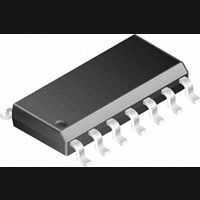
LMC6464AIM National Semiconductor, LMC6464AIM Datasheet - Page 5

LMC6464AIM
Manufacturer Part Number
LMC6464AIM
Description
Operational Amplifier (Op-Amp) IC
Manufacturer
National Semiconductor
Specifications of LMC6464AIM
No. Of Amplifiers
4
Slew Rate
0.015V/µs
No. Of Pins
14
Operating Temperature Range
-40°C To +85°C
Peak Reflow Compatible (260 C)
No
Leaded Process Compatible
No
Mounting Type
Surface Mount
Lead Free Status / RoHS Status
Contains lead / RoHS non-compliant
Available stocks
Company
Part Number
Manufacturer
Quantity
Price
Part Number:
LMC6464AIM
Manufacturer:
NS/国半
Quantity:
20 000
Company:
Part Number:
LMC6464AIMX
Manufacturer:
Texas Instruments
Quantity:
5
Part Number:
LMC6464AIMX
Manufacturer:
NS/国半
Quantity:
20 000
Company:
Part Number:
LMC6464AIMX/NOPB
Manufacturer:
Texas Instruments
Quantity:
2 700
SR
GBW
Symbol
3V AC Electrical Characteristics
Unless otherwise specified, V
tremes.
Note 1: Absolute Maximum Ratings indicate limits beyond which damage to the device may occur. Operating Ratings indicate conditions for which the device is
intended to be functional, but specific performance is not guaranteed. For guaranteed specifications and the test conditions, see the Electrical Characteristics.
Note 2: Human body model, 1.5 kΩ in series with 100 pF. All pins rated per method 3015.6 of MIL-STD-883. This is a class 2 device rating.
Note 3: Applies to both single supply and split-supply operation. Continuous short circuit operation at elevated ambient temperature can result in exceeding the
maximum allowed junction temperature of 150˚C. Output currents in excess of
Note 4: The maximum power dissipation is a function of T
P
Note 5: Typical Values represent the most likely parametric norm.
Note 6: All limits are guaranteed by testing or statistical analysis.
Note 7: V
Note 8: Do not short circuit output to V
Note 9: V
Note 10: Input referred, V
Note 11: Connected as Voltage Follower with 2V step input. Number specified is the slower of either the positive or negative slew rates.
Note 12: Limiting input pin current is only necessary for input voltages that exceed absolute maximum input voltage ratings.
Note 13: Guaranteed limits are dictated by tester limitations and not device performance. Actual performance is reflected in the typical value.
Note 14: For guaranteed Military Temperature Range parameters see RETSMC6462/4X.
D
= (T
J(MAX)
+
+
= 15V, V
= 15V. Connected as Voltage Follower with 10V step input. Number specified is the slower of either the positive or negative slew rates.
Slew Rate
Gain-Bandwidth Product
− T
A
)/θ
CM
JA
. All numbers apply for packages soldered directly into a PC board.
Parameter
= 7.5V and R
+
= 15V and R
+
L
+
= 3V, V
connected to 7.5V. For Sourcing tests, 7.5V ≤ V
, when V
L
= 100 kΩ connected to 7.5V. Each amp excited in turn with 1 kHz to produce V
+
−
is greater than 13V or reliability will be adversely affected.
(Note 11)
= 0V, V
Conditions
CM
J(MAX)
= V
, θ
JA
O
, and T
= V
(Note 5)
+
Typ
±
23
50
/2 and R
5
30 mA over long term may adversely affect reliability.
A
. The maximum allowable power dissipation at any ambient temperature is
O
≤ 11.5V. For Sinking tests, 3.5V ≤ V
L
LMC6462AI
LMC6464AI
>
(Note 6)
1M. Boldface limits apply at the temperature ex-
Limit
LMC6462BI
LMC6464BI
(Note 6)
Limit
O
= 12 V
O
≤ 7.5V.
LMC6462AM
LMC6464AM
PP
.
(Note 6)
Limit
www.national.com
Units
V/ms
kHz


