LMC6484AIM National Semiconductor, LMC6484AIM Datasheet
LMC6484AIM
Specifications of LMC6484AIM
Available stocks


Related parts for LMC6484AIM

LMC6484AIM Summary of contents
Page 1
... See the LMC6482 data sheet for a Dual CMOS operational amplifier with these same features. 3V Single Supply Buffer Circuit Rail-to-Rail Input DS011714-1 © 2000 National Semiconductor Corporation Features (Typical unless otherwise noted) n Rail-to-Rail Input Common-Mode Voltage Range (Guaranteed Over Temperature) n Rail-to-Rail Output Swing (within supply rail, ...
Page 2
... Absolute Maximum Ratings If Military/Aerospace specified devices are required, please contact the National Semiconductor Sales Office/ Distributors for availability and specifications. ESD Tolerance (Note 2) Differential Input Voltage Voltage at Input/Output Pin + − Supply Voltage (V − Current at Input Pin (Note 12) Current at Output Pin (Notes 3, 8) Current at Power Supply Pin Lead Temp ...
Page 3
DC Electrical Characteristics Unless otherwise specified, all limits guaranteed for T limits apply at the temperature extremes. Symbol Parameter V Output Swing Output Short Circuit Sourcing Current V+ ...
Page 4
AC Electrical Characteristics Unless otherwise specified, all limits guaranteed for T limits apply at the temperature extremes. Symbol Parameter T.H.D. Total Harmonic Distortion DC Electrical Characteristics Unless otherwise specified, all limits guaranteed for T Symbol Parameter V Input Offset Voltage ...
Page 5
AC Electrical Characteristics Note 3: Applies to both single supply and split-supply operation. Continuous short circuit operation at elevated ambient temperature can result in exceeding the maxi- mum allowed junction temperature of 150˚C. Output currents in excess of Note 4: ...
Page 6
Typical Performance Characteristics specified (Continued) Sinking Current vs Output Voltage DS011714-45 Input Voltage Noise vs Frequency Input Voltage Noise vs Input Voltage DS011714-50 www.national.com V = +15V, Single Supply Sinking Current vs Output Voltage DS011714-46 Input Voltage Noise ...
Page 7
Typical Performance Characteristics specified (Continued) Crosstalk Rejection vs Frequency DS011714-53 CMRR vs Frequency DS011714-56 CMRR vs Input Voltage DS011714- +15V, Single Supply Positive PSRR vs Frequency DS011714-54 CMRR vs Input Voltage DS011714- CMR OS ...
Page 8
Typical Performance Characteristics specified (Continued) Input Voltage vs Output Voltage DS011714-62 Open Loop Frequency Response DS011714-65 Gain and Phase vs Capacitive Load DS011714-68 www.national.com V = +15V, Single Supply Input Voltage vs Output Voltage DS011714-63 Open Loop Frequency ...
Page 9
Typical Performance Characteristics specified (Continued) Open Loop Output Impedance vs Frequency DS011714-71 Non-Inverting Large Signal Pulse Response DS011714-74 Non-Inverting Small Signal Pulse Response DS011714- +15V, Single Supply Slew Rate vs Supply Voltage DS011714-72 Non-Inverting Large Signal ...
Page 10
Typical Performance Characteristics specified (Continued) Inverting Large Signal Pulse Response DS011714-80 Inverting Small Signal Pulse Response DS011714-83 Stability vs Capacitive Load DS011714-86 www.national.com V = +15V, Single Supply Inverting Large Signal Pulse Response DS011714-81 Inverting Small Signal Pulse ...
Page 11
Typical Performance Characteristics specified (Continued) Stability vs Capacitive Load Application Information 1.0 Amplifier Topology The LMC6484 incorporates specially wide-compliance range current mirrors and the body effect to extend input common mode range to each supply rail. Complementary paralleled differential input ...
Page 12
Application Information loading reduces the phase margin of op-amps. The combi- nation of the op-amp’s output impedance and the capacitive load induces phase lag. This results in either an under- damped pulse response or oscillation. Capacitive load compensation can be ...
Page 13
Application Information of the ultra-low input current of the LMC6484, typically less than 20 fA essential to have an excellent layout. Fortu- nately, the techniques of obtaining low leakages are quite simple. First, the user must not ignore ...
Page 14
Application Information 7.0 Offset Voltage Adjustment Offset voltage adjustment circuits are illustrated in Figures 13 Large value resistances and potentiometers are used to reduce power consumption while providing typically mV of adjustment range, referred to the input, for ...
Page 15
Application Information 10.0 Instrumentation Circuits The LMC6484 has the high input impedance, large common-mode range and high CMRR needed for designing instrumentation circuits. Instrumentation circuits designed with the LMC6484 can reject a common-mode signals than most in-amps. This makes in- ...
Page 16
... Contact your local National Semiconductor sales office to obtain an operational amplifier spice model library disk. Typical Single-Supply Applications FIGURE 17. Half-Wave Rectifier with Input Current Protection (RI) www ...
Page 17
Typical Single-Supply Applications FIGURE 21. Large Compliance Range Current Source (Continued) FIGURE 20. Full Wave Rectifier Waveform DS011714-35 DS011714-36 FIGURE 22. Positive Supply Current Sense 17 DS011714-34 www.national.com ...
Page 18
Typical Single-Supply Applications FIGURE 23. Low Voltage Peak Detector with Rail-to-Rail Peak Capture Range In Figure 23 dielectric absorption and leakage is minimized by using a polystyrene or polyethylene hold capacitor. The droop rate is primarily determined by the value ...
Page 19
... Molded DIP 14-pin Small Outline 14-pin Ceramic LMC6484AMJ/883 DIP DS011714-4 Temperature Range Military Industrial −40˚C to +85˚C LMC6484AIN LMC6484IN LMC6484AIM, AIMX LMC6484IM, IMX 19 NSC Transport Drawing Media N14A Rail M14A Rail Tape and Reel J14A Rail ...
Page 20
Physical Dimensions www.national.com inches (millimeters) unless otherwise noted 14-Pin Ceramic Dual-In-Line Package Order Number LMC6484AMJ/883 NS Package Number J14A 20 ...
Page 21
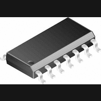
... Physical Dimensions inches (millimeters) unless otherwise noted (Continued) Order Package Number LMC6484AIM, LMC6484AIMX, LMC6484IM or LMC6484IMX 14-Pin Small Outline NS Package Number M14A 21 www.national.com ...
Page 22
... NATIONAL’S PRODUCTS ARE NOT AUTHORIZED FOR USE AS CRITICAL COMPONENTS IN LIFE SUPPORT DEVICES OR SYSTEMS WITHOUT THE EXPRESS WRITTEN APPROVAL OF THE PRESIDENT AND GENERAL COUNSEL OF NATIONAL SEMICONDUCTOR CORPORATION. As used herein: 1. Life support devices or systems are devices or systems which, (a) are intended for surgical implant ...