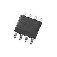
LMV822MM National Semiconductor, LMV822MM Datasheet - Page 15

LMV822MM
Manufacturer Part Number
LMV822MM
Description
Operational Amplifier (Op-Amp) IC
Manufacturer
National Semiconductor
Datasheet
1.LMV822MM.pdf
(24 pages)
Specifications of LMV822MM
No. Of Amplifiers
1
Bandwidth
5MHz
Slew Rate
1.4V/µs
No. Of Pins
8
Peak Reflow Compatible (260 C)
No
Single Supply Voltage Min (+v)
2.7V
Input Offset Voltage Max
3.5mV
Lead Free Status / RoHS Status
Contains lead / RoHS non-compliant
Available stocks
Company
Part Number
Manufacturer
Quantity
Price
Company:
Part Number:
LMV822MM
Manufacturer:
NSC
Quantity:
20 000
Company:
Part Number:
LMV822MM
Manufacturer:
NATIONAL
Quantity:
1 860
Company:
Part Number:
LMV822MM
Manufacturer:
NS
Quantity:
14 013
Company:
Part Number:
LMV822MM
Manufacturer:
NSC
Quantity:
9 500
Company:
Part Number:
LMV822MM
Manufacturer:
TOSHIBA
Quantity:
177
Part Number:
LMV822MM
Manufacturer:
NS/国半
Quantity:
20 000
Part Number:
LMV822MM/NOPB
Manufacturer:
TI/德州仪器
Quantity:
20 000
Company:
Part Number:
LMV822MM/NOPB
Manufacturer:
NSC
Quantity:
10 669
Part Number:
LMV822MMX
Manufacturer:
TI/德州仪器
Quantity:
20 000
Company:
Part Number:
LMV822MMX/NOPB
Manufacturer:
NSC
Quantity:
19 923
2.5 Tri-level Voltage Detector
The tri-level voltage detector of Figure 13 provides a type of
window comparator function. It detects three different input
voltage ranges: Min-range, Mid-range, and Max-range. The
output voltage (V
clamped at GND for the Mid-range. For the Max-range, V
at V
the circuit of Figure 13 .
Its operation is as follows: V
the diode bridge to absorb I
tion (V
ode bridge. When this limit is reached, the clamping effect
ee
. Figure 14 shows a V
O
= 0V). Eventually, I
FIGURE 13. Tri-level Voltage Detector
O
) is at V
IN
IN
O
reaches the bias limit of the di-
I
CC
to maintain a clamped condi-
vs. V
deviating from GND, causes
for the Min-range. V
I
oscilloscope photo per
DS100128-34
O
O
is
is
15
stops and the op amp responds open loop. The design equa-
tion directly preceding Figure 14 , shows how to determine
the clamping range. The equation solves for the input volt-
age band on each side GND. The mid-range is twice this
voltage band.
FIGURE 14. X, Y Oscilloscope Trace showing V
OV
V
IN
-V IN
per the Circuit of Figure 13
|
v
OV
|
DS100128-89
v
|
+V IN
DS100128-35
www.national.com
OUT
vs


