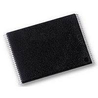
S29AL004D70TFI010 Spansion Inc., S29AL004D70TFI010 Datasheet - Page 29

S29AL004D70TFI010
Manufacturer Part Number
S29AL004D70TFI010
Description
Flash Memory IC
Manufacturer
Spansion Inc.
Datasheet
1.S29AL004D70TAI020.pdf
(55 pages)
Specifications of S29AL004D70TFI010
Memory Size
4Mbit
Memory Configuration
512K X 8 / 256K X 16
Ic Interface Type
Parallel
Access Time
70ns
Memory Case Style
TSOP
No. Of Pins
48
Operating Temperature Range
-40°C To +85°C
Lead Free Status / RoHS Status
Lead free / RoHS Compliant
Available stocks
Company
Part Number
Manufacturer
Quantity
Price
Company:
Part Number:
S29AL004D70TFI010
Manufacturer:
SPANSION
Quantity:
5 530
Company:
Part Number:
S29AL004D70TFI010
Manufacturer:
SPANSION
Quantity:
1 690
Company:
Part Number:
S29AL004D70TFI010
Manufacturer:
SPANSION
Quantity:
6 250
Company:
Part Number:
S29AL004D70TFI010H
Manufacturer:
SPANSION
Quantity:
50
February 18, 2005 S29AL004D_00_A1
RY/BY#: Ready/Busy#
The RY/BY# is a dedicated, open-drain output pin that indicates whether an Em-
bedded Algorithm is in progress or complete. The RY/BY# status is valid after the
rising edge of the final WE# pulse in the command sequence. Since RY/BY# is an
open-drain output, several RY/BY# pins can be tied together in parallel with a
pull-up resistor to V
A d v a n c e
Notes:
1. VA = Valid address for programming. During a sector
2. DQ7 should be rechecked even if DQ5 = 1 because
No
erase operation, a valid address is an address within
any sector selected for erasure. During chip erase, a
valid address is any non-protected sector address.
DQ7 may change simultaneously with DQ5.
CC
.
Figure 5. Data# Polling Algorithm
Read DQ7–DQ0
Read DQ7–DQ0
I n f o r m a t i o n
DQ7 = Data?
DQ7 = Data?
Addr = VA
Addr = VA
DQ5 = 1?
START
FAIL
S29AL004D
No
Yes
No
Yes
Yes
PASS
27


