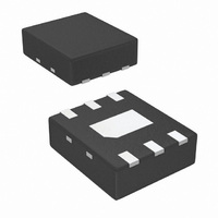
LM26LVCISD-105/NOPB National Semiconductor, LM26LVCISD-105/NOPB Datasheet - Page 15

LM26LVCISD-105/NOPB
Manufacturer Part Number
LM26LVCISD-105/NOPB
Description
IC TEMP SENS/SWITCH 105C 6LLP
Manufacturer
National Semiconductor
Series
PowerWise®r
Datasheet
1.LM26LVEB.pdf
(20 pages)
Specifications of LM26LVCISD-105/NOPB
Sensing Temperature
105°C Trip Point
Output Type
Active High/Push Pull, Active Low/Open Drain, Voltage
Voltage - Supply
1.6 V ~ 5.5 V
Accuracy
±2.2°C
Package / Case
6-WDFN Exposed Pad
Lead Free Status / RoHS Status
Lead free / RoHS Compliant
Other names
LM26LVCISD-105TR
2.0 OVERTEMP and OVERTEMP
Digital Outputs
The OVERTEMP Active High, Push-Pull Output and the
OVERTEMP Active Low, Open-Drain Output both assert at
the same time whenever the Die Temperature reaches the
factory preset Temperature Trip Point. They also assert si-
multaneously whenever the TRIP TEST pin is set high. Both
outputs de-assert when the die temperature goes below the
Temperature Trip Point - Hysteresis. These two types of dig-
ital outputs enable the user the flexibility to choose the type
of output that is most suitable for his design.
Either the OVERTEMP or the OVERTEMP Digital Output pins
can be left open if not used.
2.1 OVERTEMP OPEN-DRAIN DIGITAL OUTPUT
The OVERTEMP Active Low, Open-Drain Digital Output, if
used, requires a pull-up resistor between this pin and V
The following section shows how to determine the pull-up re-
sistor value.
Determining the Pull-up Resistor Value
The Pull-up resistor value is calculated at the condition of
maximum total current, i
rent is:
where,
i
i
V
V
The pull-up resistor maximum value can be found by using
the following formula:
EXAMPLE CALCULATION
Suppose we have, for our example, a V
CMOS digital input as a load, a V
T
L
OUT
DD(Max)
i
Resistor at V
i
digital inputs.
V
V
V
used in the customer's system.
T
L
OUT
OL
DD(Max)
is the maximum total current through the Pull-up
is the load current, which is very low for typical
for calculating the Pull-up resistor.
is the Voltage at the OVERTEMP pin. Use
is the maximum power supply voltage to be
OL
T
.
, through the resistor. The total cur-
OL
of 0.2 V.
DD
of 3.3 V ± 0.3V, a
20204752
DD
.
15
(1) We see that for V
OVERTEMP shows a maximim i
(2) Let i
35 µA as the current limit then i
35 µA
(3) We notice that V
calculate the pull-up resistor as
R
(4) Based on this calculated value, we select the closest re-
sistor value in the tolerance family we are using.
In our example, if we are using 5% resistor values, then the
next closest value is 100 kΩ.
2.2 NOISE IMMUNITY
The LM26LV is virtually immune from false triggers on the
OVERTEMP and OVERTEMP digital outputs due to noise on
the power supply. Test have been conducted showing that,
with the die temperature within 0.5°C of the temperature trip
point, and the severe test of a 3 Vpp square wave "noise"
signal injected on the V
5V, there were no false triggers.
3.0 TRIP TEST Digital Input
The TRIP TEST pin simply provides a means to test the
OVERTEMP and OVERTEMP digital outputs electronically
by causing them to assert, at any operating temperature, as
a result of forcing the TRIP TEST pin high.
When the TRIP TEST pin is pulled high the V
at the V
If not used, the TRIP TEST pin may either be left open or
grounded.
4.0 V
Sensor Output
The V
source significant current. This is beneficial when, for exam-
ple, driving dynamic loads like an input stage on an analog-
to-digital converter (ADC). In these applications the source
current is required to quickly charge the input capacitor of the
ADC. See the Applications Circuits section for more discus-
sion of this topic. The LM26LV is ideal for this and other
applications which require strong source or sink current.
4.1 NOISE CONSIDERATIONS
The LM26LV's supply-noise rejection (the ratio of the AC sig-
nal on V
bench tests. It's typical attenuation is shown in the Typical
Performance Characteristics section. A load capacitor on the
output can help to filter noise.
For operation in very noisy environments, some bypass ca-
pacitance should be present on the supply within approxi-
mately 2 inches of the LM26LV.
4.2 CAPACITIVE LOADS
The V
tremely noisy environment, or when driving a switched sam-
pling input on an ADC, it may be necessary to add some
filtering to minimize noise coupling. Without any precautions,
the V
1100 pF as shown in
than 1100 pF, a series resistor is required on the output, as
shown in
Pull-up
TEMP
TEMP
TEMP
= (3.6 − 0.2)/35 µA = 97k
TRIP
L
TEMP
TEMP
= 1 µA, then i
Figure
can drive a capacitive load less than or equal to
Output handles capacitive loading well. In an ex-
push-pull output provides the ability to sink and
voltage.
to the AC signal on V
Analog Temperature
2, to maintain stable conditions.
OL
DD(Max)
Figure
of 0.2 V the electrical specification for
T
DD
is about 386 µA max. If we select
line, over the V
is 3.3V + 0.3V = 3.6V and then
1. For capacitive loads greater
T
sink
for the calculation becomes
DD
of 385 µA.
) was measured during
DD
TEMP
range of 2V to
www.national.com
pin will be


