MV2105G ON Semiconductor, MV2105G Datasheet
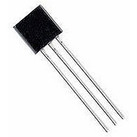
VARICAP DIODE, 16.5PF, 0.1UA, TO-92

MV2105G

Manufacturer Part Number
MV2105G
Description
VARICAP DIODE, 16.5PF, 0.1UA, TO-92
Manufacturer
ON Semiconductor
Datasheet

Specifications of MV2105G

Capacitance Cd Max @ Vr F
16.5pF
Q @ Vr F
400
Forward Current If(av)
200mA
Repetitive Reverse Voltage Vrrm Max
30V
Diode Case Style
TO-92
No. Of Pins
2
Mounting Type
Through Hole
Configuration
Single
Operating Temperature Classification
Military
Pin Count
2
Breakdown Voltage
30V
Rohs Compliant
Yes
Lead Free Status / RoHS Status
Lead free / RoHS Compliant
Lead Free Status / RoHS Status
Lead free / RoHS Compliant
MMBV2101LT1 Series,
MV2105, MV2101, MV2109,
LV2209
Silicon Tuning Diodes
volume requirements of FM Radio and TV tuning and AFC, general
frequency control and tuning applications. They provide solid−state
reliability in replacement of mechanical tuning methods. Also
available in a Surface Mount Package up to 33 pF.
Features
Maximum ratings are those values beyond which device damage can occur.
Maximum ratings applied to the device are individual stress limit values (not
normal operating conditions) and are not valid simultaneously. If these limits are
exceeded, device functional operation is not implied, damage may occur and
reliability may be affected.
© Semiconductor Components Industries, LLC, 2006
January, 2006 − Rev. 4
MAXIMUM RATINGS
ELECTRICAL CHARACTERISTICS
Reverse Voltage
Forward Current
Forward Power Dissipation
@ T
Derate above 25°C
@ T
Derate above 25°C
Junction Temperature
Storage Temperature Range
Reverse Breakdown Voltage
(I
Reverse Voltage Leakage Current
(V
Diode Capacitance Temperature Co-
efficient (V
These devices are designed in popular plastic packages for the high
R
High Q
Controlled and Uniform Tuning Ratio
Standard Capacitance Tolerance − 10%
Complete Typical Design Curves
Pb−Free Packages are Available
R
= 10 mAdc)
A
A
= 25 Vdc, T
= 25°C
= 25°C
Characteristic
R
= 4.0 Vdc, f = 1.0 MHz)
Rating
MMBV21xx, MV21xx
A
= 25°C)
MMBV21xx
MV21xx
LV2209
LV2209
Preferred Device
Symbol
Symbol
V
TC
T
(BR)R
V
P
T
I
I
stg
(T
R
F
R
D
J
C
A
= 25°C unless otherwise noted)
Min
30
25
−55 to +150
Value
+150
200
225
280
Typ
280
1.8
2.8
30
Max
0.1
1
mW/°C
mW/°C
ppm/°C
mAdc
mAdc
Unit
Unit
Vdc
mW
mW
Vdc
°C
°C
See detailed ordering and shipping information in the package
dimensions section on page 2 of this data sheet.
Preferred devices are recommended choices for future use
and best overall value.
1
1
*Date Code orientation and/or overbar may
vary depending upon manufacturing location.
(Note: Microdot may be in either location)
2
2
CAPACITANCE DIODES
6.8−100 pF, 30 VOLTS
VOLTAGE VARIABLE
yyyyyy = Specific Device Code
A
Y
WW
G
ORDERING INFORMATION
3
xxx = Specific Device Code
M
G
TO−92 (TO−226AC)
SOT−23 (TO−236)
Cathode
Cathode
CASE 318−08
http://onsemi.com
= Date Code*
= Pb−Free Package
CASE 182
3
2
STYLE 8
STYLE 1
= Assembly Location
= Year
= Work Week
= Pb−Free Package
SOT−23
TO−92
Publication Order Number:
Anode
Anode
MMBV2101LT1/D
1
1
1
DIAGRAMS
MARKING
AYWW G
xxx M G
yyyy
yy
G
G

Related parts for MV2105G

MV2105G Summary of contents

Page 1

MMBV2101LT1 Series, MV2105, MV2101, MV2109, LV2209 Preferred Device Silicon Tuning Diodes These devices are designed in popular plastic packages for the high volume requirements of FM Radio and TV tuning and AFC, general frequency control and tuning applications. They provide ...

Page 2

... MV2101G MV2101 TO−92 (Pb−Free) MMBV2103LT1 4H SOT−23 MMBV2105LT1 4U SOT−23 MMBV2105LT1G 4U SOT−23 (Pb−Free) MMBV2105L 4U SOT−23 MV2105 MV2105 TO−92 MV2105G MV2105 TO−92 (Pb−Free) MMBV2107LT1 4W SOT−23 MMBV2107LT1G 4W SOT−23 (Pb−Free) MMBV2107L 4W SOT−23 MMBV2108LT1 4X SOT−23 MMBV2108LT1G 4X SOT−23 (Pb−Free) ...

Page 3

MMBV2101LT1 Series, MV2105, MV2101, MV2109, LV2209 TYPICAL DEVICE CHARACTERISTICS 1000 500 200 MMBV2109LT1/MV2109 100 50 MMBV2105LT1/MV2105 20 MMBV2101LT1/MV2101 10 5.0 2.0 1.0 0.5 0.1 0.2 0.3 Figure 1. Diode Capacitance versus Reverse Voltage 1.040 1.030 1.020 1.010 1.000 0.990 NORMALIZED ...

Page 4

... *For additional information on our Pb−Free strategy and soldering details, please download the ON Semiconductor Soldering and Mounting Techniques Reference Manual, SOLDERRM/D. PACKAGE DIMENSIONS SOT−23 (TO−236) CASE 318−08 ISSUE AN NOTES: 1. DIMENSIONING AND TOLERANCING PER ANSI Y14.5M, 1982. 2. CONTROLLING DIMENSION: INCH. 3. MAXIMUM LEAD THICKNESS INCLUDES LEAD FINISH THICKNESS ...

Page 5

... J K SECTION X− American Technical Support: 800−282−9855 Toll Free USA/Canada Japan: ON Semiconductor, Japan Customer Focus Center 2−9−1 Kamimeguro, Meguro−ku, Tokyo, Japan 153−0051 Phone: 81−3−5773−3850 http://onsemi.com 5 NOTES: 1. DIMENSIONING AND TOLERANCING PER ANSI Y14 ...

Related keywords