2N5116JANTX Vishay, 2N5116JANTX Datasheet
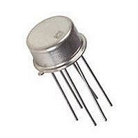
P CHANNEL JFET, 30V, TO-206AA

2N5116JANTX

Manufacturer Part Number
2N5116JANTX
Description
P CHANNEL JFET, 30V, TO-206AA
Manufacturer
Vishay
Datasheets

Specifications of 2N5116JANTX

Breakdown Voltage Vbr
30V
Gate-source Cutoff Voltage Vgs(off) Max
4V
Power Dissipation Pd
500mW
Operating Temperature Range
-55°C To +200°C
No. Of Pins
3
Mounting Type
Through Hole
Leaded Process Compatible
No
Rohs Compliant
No
Lead Free Status / RoHS Status
Contains lead / RoHS non-compliant
The 2N5114 series consists of p-channel JFET analog
switches designed to provide low on-resistance, good
off-isolation, and fast switching. These JFETs are optimized
for use in complementary switching applications with the
Vishay Siliconix 2N4856A series.
Gate-Drain Voltage
Gate-Source Voltage
Gate Current
Storage Temperature
Operating Junction Temperature
For applications information see AN104.
Document Number: 70260
S-04030—Rev. E, 04-Jun-01
D Low On-Resistance: 2N5114 <75 W
D Fast Switching—t
D High Off-Isolation—I
D Low Capacitance: 6 pF
D Low Insertion Loss
Part Number
2N5114
2N5115
2N5116
. . . . . . . . . . . . . . . . . . . . . . . . . . . . . . . . . . . . . . . . . . . . . . . .
. . . . . . . . . . . . . . . . . . . . . . . . . . . . . . . . . . . . . . . . . . . . .
. . . . . . . . . . . . . . . . . . . . . . . . . . . . . . . . . . . . . . . . . . . .
. . . . . . . . . . . . . . . . . . . . . . . . . . . . . . . . . . .
V
ON
GS(off)
: 16 ns
D(off)
5 to 10
3 to 6
1 to 4
. . . . . . . . . . . . . . . . . . . . . . . . . .
: –10 pA
(V)
r
DS(on)
100
150
75
Max (W)
Case
P-Channel JFETs
D Low Error Voltage
D High-Speed Analog Circuit Performance
D Negligible “Off-Error,” Excellent Accuracy
D Good Frequency Response
D Eliminates Additional Buffering
–65 to 200_C
–55 to 200_C
G
S
–50 mA
1
2
30 V
30 V
TO-206AA
I
D(off)
Top View
(TO-18)
Typ (pA)
–10
–10
–10
3
The 2N5114 series is available with JAN, JANTX, or JANTXV
level processing, (see 2N5114 JAN series data sheet).
Lead Temperature (
Power Dissipation
Notes
a.
D
Derate 3 mW/_C above 25_C
t
ON
Max (ns)
a
16
30
42
1
. . . . . . . . . . . . . . . . . . . . . . . . . . . . . . . . . . . . . . . . .
/
16
” from case for 10 sec.)
2N5114/5115/5116
D Analog Switches
D Choppers
D Sample-and-Hold
D Normally “On” Switches
D Current Limiters
Vishay Siliconix
. . . . . . . . . . . . . . . . . . .
www.vishay.com
500 mW
300_C
9-1

Related parts for 2N5116JANTX

2N5116JANTX Summary of contents

Page 1

... These JFETs are optimized for use in complementary switching applications with the Vishay Siliconix 2N4856A series. Gate-Drain Voltage . . . . . . . . . . . . . . . . . . . . . . . . . . . . . . . . . . . . . . . . . . . . . ...

Page 2

... Vishay Siliconix _ Parameter Symbol Static Gate-Source V (BR)GSS Breakdown Voltage Gate-Source Cutoff Voltage V GS(off) b Saturation Drain Current I DSS Gate Reverse Current I GSS c Gate Operating Current I G Drain Cutoff Current I D(off) Drain-Source On-Voltage V DS(on) DS(on) Drain-Source r DS(on) On-Resistance Gate-Source V GS(F) Forward Voltage ...

Page 3

... Forward Transconductance and Output Conductance –100 18 I DSS –80 15 –60 12 –40 9 – 300 240 180 120 60 0 –100 – – 2N5114/5115/5116 Vishay Siliconix vs. Gate-Source Cutoff Voltage g and – kHz – Gate-Source Cutoff Voltage (V) GS(off) On-Resistance vs. Temperature I = – changes X 0.7%/ 1.5 V GS(off –35 – ...

Page 4

... Vishay Siliconix Output Characteristics – 1.5 V 0.5 V –1.6 1.0 V –1.2 –0.8 –0 –0.1 –0.2 –0.3 V – Drain-Source Voltage (V) DS Output Characteristics – GS(off) –20 –15 –10 – –4 –8 –12 V – Drain-Source Voltage (V) DS Capacitance vs. Gate-Source Voltage MHz iss 12 C rss ...

Page 5

... S-04030—Rev. E, 04-Jun-01 _ – – –32 –24 –16 –8 0.8 1.0 100 V = – 2N5116 – GS( 390 W V GS(L) – –5 V 2N5114/5115/5116 Vishay Siliconix Transfer Characteristics –15 V GS(off –55_C A 25_C 125_C – Gate-Source Voltage (V) GS Noise Voltage vs. Frequency I = –0 – – 100 ...

Related keywords