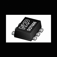
2N7002BKV NXP Semiconductors, 2N7002BKV Datasheet

2N7002BKV
Specifications of 2N7002BKV
Available stocks
Related parts for 2N7002BKV
2N7002BKV Summary of contents
Page 1
... V, 340 mA dual N-channel Trench MOSFET Rev. 2 — 22 September 2010 1. Product profile 1.1 General description Dual N-channel enhancement mode Field-Effect Transistor (FET ultra small SOT666 Surface-Mounted Device (SMD) plastic package using Trench MOSFET technology. 1.2 Features and benefits Logic-level compatible ...
Page 2
... T amb drain current amb T amb = 25 °C; peak drain current T amb single pulse; t All information provided in this document is subject to legal disclaimers. Rev. 2 — 22 September 2010 2N7002BKV 60 V, 340 mA dual N-channel Trench MOSFET Simplified outline Graphic symbol Marking code ZG Min - - [ ° 100 ° ...
Page 3
... T amb junction temperature ambient temperature storage temperature 017aaa001 75 125 175 T (°C) amb Fig 2. All information provided in this document is subject to legal disclaimers. Rev. 2 — 22 September 2010 2N7002BKV 60 V, 340 mA dual N-channel Trench MOSFET Min = 25 °C [ °C [ °C [2] - −55 − ...
Page 4
... All information provided in this document is subject to legal disclaimers. Rev. 2 — 22 September 2010 2N7002BKV 60 V, 340 mA dual N-channel Trench MOSFET 10 V (V) DS Min Typ [1] - ...
Page 5
... Fig 5. Transient thermal impedance from junction to ambient as a function of pulse duration; typical values 2N7002BKV Product data sheet 60 V, 340 mA dual N-channel Trench MOSFET − − All information provided in this document is subject to legal disclaimers. Rev. 2 — 22 September 2010 2N7002BKV 017aaa060 (s) p 017aaa061 (s) p © ...
Page 6
... V GS turn-off delay time R G fall time source-drain voltage I S ≤ 300 μs; δ ≤ 0.01. p All information provided in this document is subject to legal disclaimers. Rev. 2 — 22 September 2010 2N7002BKV 60 V, 340 mA dual N-channel Trench MOSFET Min = 10 μ 250 μ 1 ° ...
Page 7
... V 3.0 4.0 V (V) DS Fig 7. 017aaa041 R (2) (3) (4) (5) 0.6 0.8 1.0 I (A) D Fig 9. All information provided in this document is subject to legal disclaimers. Rev. 2 — 22 September 2010 2N7002BKV 60 V, 340 mA dual N-channel Trench MOSFET − (A) −4 10 (1) (2) (3) −5 10 −6 10 0.0 1.0 2 ° ...
Page 8
... Fig 11. Normalized drain-source on-state resistance 017aaa045 120 180 T (°C) amb Fig 13. Input, output and reverse transfer All information provided in this document is subject to legal disclaimers. Rev. 2 — 22 September 2010 2N7002BKV 60 V, 340 mA dual N-channel Trench MOSFET 2.4 a 1.8 1.2 0.6 0.0 −60 0 ...
Page 9
... Q (nC °C amb Fig 15. Gate charge waveform definitions 1 (A) 0.8 (1) 0.4 0.0 0.0 0.4 All information provided in this document is subject to legal disclaimers. Rev. 2 — 22 September 2010 2N7002BKV 60 V, 340 mA dual N-channel Trench MOSFET GS(pl) V GS(th GS1 GS2 G(tot) ...
Page 10
... NXP Semiconductors 8. Test information Fig 17. Duty cycle definition 2N7002BKV Product data sheet 60 V, 340 mA dual N-channel Trench MOSFET P duty cycle δ All information provided in this document is subject to legal disclaimers. Rev. 2 — 22 September 2010 2N7002BKV 006aaa812 © NXP B.V. 2010. All rights reserved ...
Page 11
... 1.3 1.7 0.3 1.0 0.5 1.1 1.5 0.1 REFERENCES JEDEC JEITA All information provided in this document is subject to legal disclaimers. Rev. 2 — 22 September 2010 2N7002BKV 60 V, 340 mA dual N-channel Trench MOSFET detail 0.1 0.1 EUROPEAN PROJECTION SOT666 X ISSUE DATE 04-11-08 06-03-16 © NXP B.V. 2010. All rights reserved. ...
Page 12
... Reflow soldering is the only recommended soldering method. All information provided in this document is subject to legal disclaimers. Rev. 2 — 22 September 2010 2N7002BKV 60 V, 340 mA dual N-channel Trench MOSFET 0.4 0.3 0.25 (6×) (2×) (2×) 0.325 0.375 Dimensions in mm (4× ...
Page 13
... NXP Semiconductors 11. Revision history Table 8. Revision history Document ID Release date 2N7002BKV v.2 20100922 • Modifications: Table 2 • Table 6 “Thermal • Table 6 “Thermal 2N7002BKV v.1 20100610 2N7002BKV Product data sheet 60 V, 340 mA dual N-channel Trench MOSFET Data sheet status Product data sheet “ ...
Page 14
... Export control — This document as well as the item(s) described herein may be subject to export control regulations. Export might require a prior authorization from national authorities. All information provided in this document is subject to legal disclaimers. Rev. 2 — 22 September 2010 2N7002BKV © NXP B.V. 2010. All rights reserved ...
Page 15
... Trademarks Notice: All referenced brands, product names, service names and trademarks are the property of their respective owners. http://www.nxp.com salesaddresses@nxp.com All information provided in this document is subject to legal disclaimers. Rev. 2 — 22 September 2010 2N7002BKV © NXP B.V. 2010. All rights reserved ...
Page 16
... Please be aware that important notices concerning this document and the product(s) described herein, have been included in section ‘Legal information’. © NXP B.V. 2010. For more information, please visit: http://www.nxp.com For sales office addresses, please send an email to: salesaddresses@nxp.com All rights reserved. Date of release: 22 September 2010 Document identifier: 2N7002BKV ...


