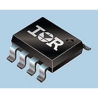
IRF7501PBF International Rectifier, IRF7501PBF Datasheet

IRF7501PBF
Specifications of IRF7501PBF
Related parts for IRF7501PBF
IRF7501PBF Summary of contents
Page 1
... Operating Junction and Storage Temperature Range Soldering Temperature, for 10 seconds Thermal Resistance Parameter Maximum Junction-to-Ambient „ R θJA All Micro8 Data Sheets reflect improved Thermal Resistance, Power and Current -Handling Ratings- effective only for product marked with Date Code 505 or later . www.irf.com IRF7501PbF HEXFET ...
Page 2
... IRF7501PbF Electrical Characteristics @ T Parameter V Drain-to-Source Breakdown Voltage (BR)DSS ∆V Breakdown Voltage Temp. Coefficient /∆T (BR)DSS J R Static Drain-to-Source On-Resistance DS(on) V Gate Threshold Voltage GS(th) g Forward Transconductance fs I Drain-to-Source Leakage Current DSS Gate-to-Source Forward Leakage I GSS Gate-to-Source Reverse Leakage Q Total Gate Charge ...
Page 3
... TOP 10 BOTTOM 1.5V 1 0.1 A 0.01 0.1 10 Fig 2. Typical Output Characteristics 100 150° 10V 0.1 A 3.5 4.0 0.4 Fig 7. Typical Source-Drain Diode IRF7501PbF VGS 7.5V 5.0V 4.0V 3.5V 3.0V 2.5V 2.0V 1.5V 20µs PULSE WIDTH T = 150° Drain-to-Source Voltage ( 25° 0.6 ...
Page 4
... IRF7501PbF 2 1.7A D 1.5 1.0 0.5 0.0 -60 -40 - Junction Temperature (°C) J Fig 5. Normalized On-Resistance Vs. Temperature 0.13 0.11 0.09 0.07 0.05 4 0.8 0.6 0.4 0 4.5V 0 100 120 140 160 Fig 6. Typical On-Resistance Vs. Drain Gate-to-Source Voltage (V) GS Fig 7. Typical On-Resistance Vs. Gate 5.0V ...
Page 5
... RESPONSE) 0.1 0.00001 0.0001 Fig 10. Maximum Effective Transient Thermal Impedance, Junction-to-Ambient www.irf.com 1. SHORTED 100 0.001 0.01 0 Rectangular Pulse Duration (sec) 1 IRF7501PbF = 16V FOR TEST CIRCUIT SEE FIGURE Total Gate Charge (nC) G Fig 9. Typical Gate Charge Vs. Gate-to-Source Voltage Notes: 1. Duty factor Peak ...
Page 6
... IRF7501PbF Charge Fig 11a. Basic Gate Charge Waveform Fig 12a. Switching Time Test Circuit V DS 90% 10 Fig 12b. Switching Time Waveforms 6 12V V GS Fig 11b. Gate Charge Test Circuit + - ≤ 1 ≤ 0 d(on) r d(off) f Current Regulator Same Type as D.U.T. 50KΩ .2µF .3µ ...
Page 7
... Driver Gate Drive Period P.W. D.U.T. I Waveform SD Reverse Recovery Body Diode Forward Current D.U.T. V Waveform DS Re-Applied Voltage Body Diode Inductor Curent Ripple ≤ 5% www.irf.com • • • P. Period V GS Current di/dt Diode Recovery dv/ Forward Drop I SD IRF7501PbF + - =10V 7 ...
Page 8
... IRF7501PbF Micro8 Package Outline Dimensions are shown in milimeters (inches 0.25 (.010 0.08 (.003 NOTES: 1 DIMENSIONING AND TOLERANCING PER ANSI Y14.5M-1982. 2 CONTROLLING DIMENSION : INCH. 3 DIMENSIONS DO NOT INCLUDE MOLD FLASH. Micro8 Part Marking Information EXAMPLE: T HIS IS AN IRF7501 LOT CODE (XX) PART NUMBER WW = (1-26) IF PRECEDED BY LAS T DIGIT OF CALENDAR YEAR ...
Page 9
... IR WORLD HEADQUARTERS: 233 Kansas St., El Segundo, California 90245, USA Tel: (310) 252-7105 www.irf.com 12.3 ( .484 ) 11.7 ( .461 ) FEED DIRECTION 14.40 ( .566 ) 12.40 ( .488 ) Data and specifications subject to change without notice. Qualifications Standards can be found on IR’s Web site. TAC Fax: (310) 252-7903 Visit us at www.irf.com for sales contact information. 02/05 IRF7501PbF 9 ...


