IRF7220PBF International Rectifier, IRF7220PBF Datasheet
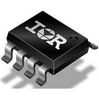
P CHANNEL MOSFET, -14V, 11A, SOIC

IRF7220PBF

Manufacturer Part Number
IRF7220PBF
Description
P CHANNEL MOSFET, -14V, 11A, SOIC
Manufacturer
International Rectifier
Datasheets

Specifications of IRF7220PBF

Transistor Polarity
P Channel
Continuous Drain Current Id
11A
Drain Source Voltage Vds
-14V
On Resistance Rds(on)
12mohm
Rds(on) Test Voltage Vgs
-4.5V
Threshold Voltage Vgs Typ
-600mV
Channel Type
P
Current, Drain
±11 A
Gate Charge, Total
84 nC
Package Type
SO-8
Polarization
P-Channel
Power Dissipation
2.5 W
Resistance, Drain To Source On
0.0082 Ohm
Temperature, Operating, Maximum
+150 °C
Temperature, Operating, Minimum
-55 °C
Time, Turn-off Delay
140 ns
Time, Turn-on Delay
19 ns
Transconductance, Forward
8.4 S
Voltage, Breakdown, Drain To Source
-14 V
Voltage, Drain To Source
–12 V
Voltage, Forward, Diode
-1.2 V
Voltage, Gate To Source
±12 V
Configuration
Single Quad Drain Triple Source
Resistance Drain-source Rds (on)
12 mOhms
Drain-source Breakdown Voltage
- 12 V
Gate-source Breakdown Voltage
12 V
Continuous Drain Current
- 11 A
Maximum Operating Temperature
+ 150 C
Mounting Style
SMD/SMT
Package / Case
SOIC-8
Fall Time
1040 ns
Gate Charge Qg
84 nC
Minimum Operating Temperature
- 55 C
Rise Time
420 ns
Lead Free Status / RoHS Status
Lead free / RoHS Compliant
Lead Free Status / RoHS Status
Lead free / RoHS Compliant

Available stocks

Company
Part Number
Manufacturer
Quantity
Price
Part Number:
IRF7220PBF
Manufacturer:
IR
Quantity:
20 000
l
l
l
l
Absolute Maximum Ratings
Thermal Resistance
Description
These P-Channel MOSFETs from International Rectifier
utilize advanced processing techniques to achieve the
extremely low on-resistance per silicon area. This benefit
provides the designer with an extremely efficient device for
use in battery and load management applications.
The SO-8 has been modified through a customized
leadframe for enhanced thermal characteristics and
multiple-die capability making it ideal in a variety of power
applications. With these improvements, multiple devices
can be used in an application with dramatically reduced
board space. The package is designed for vapor phase,
infrared, or wave soldering techniques.
www.irf.com
V
I
I
I
P
P
E
V
T
R
D
D
DM
J,
DS
D
D
AS
GS
@ T
@ T
JA
Ultra Low On-Resistance
P-Channel MOSFET
Surface Mount
Available in Tape & Reel
@T
@T
T
STG
A
A
A
A
= 70°C
= 25°C
= 25°C
= 70°C
Drain- Source Voltage
Continuous Drain Current, V
Pulsed Drain Current 
Linear Derating Factor
Single Pulse Avalanche Energy„
Gate-to-Source Voltage
Junction and Storage Temperature Range
Maximum Junction-to-Ambient
Power Dissipation
Power Dissipation
Parameter
Parameter
GS
GS
ƒ
@ -4.5V
@ -4.5V
G
S
S
S
1
2
3
4
T op V ie w
HEXFET
8
7
6
5
-55 to + 150
Max.
Max.
±8.8
0.02
D
D
D
±11
±88
110
± 12
50
D
-14
2.5
1.6
A
SO-8
®
R
IRF7220
DS(on)
Power MOSFET
V
DSS
= 0.012
PD- 91850C
= -14V
Units
Units
W/°C
°C/W
W
mJ
°C
V
A
V
1
7/16/99

Related parts for IRF7220PBF

IRF7220PBF Summary of contents

Page 1

... Surface Mount Available in Tape & Reel l Description These P-Channel MOSFETs from International Rectifier utilize advanced processing techniques to achieve the extremely low on-resistance per silicon area. This benefit provides the designer with an extremely efficient device for use in battery and load management applications. ...

Page 2

IRF7220 Electrical Characteristics @ T Parameter V Drain-to-Source Breakdown Voltage (BR)DSS Breakdown Voltage Temp. Coefficient (BR)DSS J R Static Drain-to-Source On-Resistance DS(on) V Gate Threshold Voltage GS(th) g Forward Transconductance fs I Drain-to-Source Leakage Current DSS Gate-to-Source ...

Page 3

VG S TOP - 4.5V - 4.0V - 3.0V - 2.0V - 1.8V - 1. TTO M - 1.2V 300µs PULSE W IDTH T = 25° ...

Page 4

IRF7220 0V 1kHz ...

Page 5

T , Case Temperature ( C) C Fig 9. Maximum Drain Current Vs. Case Temperature 100 D = 0.50 0.20 10 0.10 0.05 0.02 1 0.01 SINGLE PULSE (THERMAL ...

Page 6

IRF7220 SO-8 Package Details (. ...

Page 7

Tape and Reel ...

Related keywords