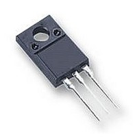
BUL312FP STMicroelectronics, BUL312FP Datasheet

BUL312FP
Specifications of BUL312FP
Available stocks
Related parts for BUL312FP
BUL312FP Summary of contents
Page 1
... HORIZONTAL DEFLECTION FOR TV SMPS ELECTRONIC BALLASTS FOR FLUORESCENT LIGHTING DESCRIPTION The BUL312FP is manufactured using high voltage Multi Epitaxial Planar technology for high switching speeds and high voltage capability. It uses a Cellular Emitter structure with planar edge termination to enhance switching speeds while maintaining a wide RBSOA. ...
Page 2
... BUL312FP THERMAL DATA R Thermal Resistance Junction-Case thj-case R Thermal Resistance Junction-Ambient thj-amb ELECTRICAL CHARACTERISTICS (T Symbol Parameter I Collector Cut-off CES Current ( Collector Cut-off CEO Current ( Collector-Emitter CEO(sus) Sustaining Voltage ( Emitter-Base Voltage EBO ( Collector-Emitter CE(sat) Saturation Voltage V Base-Emitter BE(sat) Saturation Voltage h DC Current Gain ...
Page 3
... DC Current Gain Collector Emitter Saturation Voltage Inductive Fall Time DC Current Gain Base Emitter Saturation Voltage Inductive Storage Time BUL312FP 3/6 ...
Page 4
... BUL312FP Reverse Biased SOA 4/6 Figure 1: Inductive Load Switching Test Circuit (1) Fast electronic switch (2) Non-inductive Resistor (3) Fast recovery rectifier ...
Page 5
... BUL312FP inch TYP. MAX. 0.181 0.106 0.108 0.027 0.039 0.067 0.067 0.204 0.106 0.409 0.630 1.204 0.417 0.645 0.366 0.126 5/6 ...
Page 6
... BUL312FP Information furnished is believed to be accurate and reliable. However, STMicroelectronics assumes no responsibility for the consequences of use of such information nor for any infringement of patents or other rights of third parties which may result from its use. No license is granted by implication or otherwise under any patent or patent rights of STMicroelectronics. Specification mentioned in this publication are subject to change without notice ...


