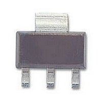
BSP149L6327 Infineon Technologies, BSP149L6327 Datasheet

BSP149L6327
Specifications of BSP149L6327
Related parts for BSP149L6327
BSP149L6327 Summary of contents
Page 1
SIPMOS Small-Signal-Transistor Features • N-channel • Depletion mode • dv /dt rated • Available with V indicator on reel GS(th) • Pb-free lead plating; RoHS compliant Type Package BSP149 PG-SOT-223 BSP149 PG-SOT-223 Maximum ratings =25 °C, unless ...
Page 2
Parameter Thermal characteristics Thermal resistance, junction - soldering point (pin 4) SMD version, device on PCB Electrical characteristics Static characteristics Drain-source breakdown voltage Gate threshold voltage Drain-source cutoff current Gate-source leakage current On-state drain current Drain-source on-state resistance ...
Page 3
Parameter Dynamic characteristics Input capacitance Output capacitance Reverse transfer capacitance Turn-on delay time Rise time Turn-off delay time Fall time Gate Charge Characteristics Gate to source charge Gate to drain charge Gate charge total Gate plateau voltage Reverse Diode Diode ...
Page 4
Power dissipation P =f(T ) tot A 2 1 [° Safe operating area I =f =25 ° parameter limited ...
Page 5
Typ. output characteristics I =f =25 ° parameter 0.8 0.6 0.4 0 Typ. transfer characteristics I =f |>2 ...
Page 6
Drain-source on-state resistance R =f =0. DS(on %98 2 typ 0 -60 - [° Threshold voltage bands I =f ...
Page 7
Forward characteristics of reverse diode I =f parameter 150 °C 1 0.12 A 150 °C, 98% 0.1 0. °C, 98 Drain-source breakdown voltage V =f(T ); ...
Page 8
Package Outline: Footprint: Dimensions in mm Rev. 1.2 Packaging: page 8 BSP149 2005-11-28 ...
Page 9
... Due to technical requirements, components may contain dangerous substances. For information on the types in question, please contact your nearest Infineon Technologies office. Infineon Technologies' components may only be used in life-support devices or systems with the expressed written approval of Infineon Technologies if a failure of such components can reasonably be expected to cause the failure of that life-support device or system affect the safety or effectiveness of that device or system ...


