FQD18N20V2 Fairchild Semiconductor, FQD18N20V2 Datasheet
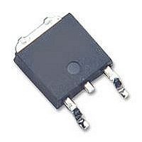
MOSFET, N, D-PAK

FQD18N20V2

Manufacturer Part Number
FQD18N20V2
Description
MOSFET, N, D-PAK
Manufacturer
Fairchild Semiconductor
Datasheet

Specifications of FQD18N20V2

Transistor Polarity
N Channel
Continuous Drain Current Id
15A
Drain Source Voltage Vds
200V
On Resistance Rds(on)
140mohm
Rds(on) Test Voltage Vgs
10V
Voltage Vgs Max
30V
Operating Temperature Range
-55°C To
Threshold Voltage Vgs Typ
5V
Rohs Compliant
Yes
Lead Free Status / RoHS Status
Lead free / RoHS Compliant

Available stocks

Company
Part Number
Manufacturer
Quantity
Price
Part Number:
FQD18N20V2
Manufacturer:
FAIRCHILD
Quantity:
12 500
Part Number:
FQD18N20V2TM
Manufacturer:
Fairchild Semiconductor
Quantity:
135
Part Number:
FQD18N20V2TM
Manufacturer:
FAIRCHILD/仙童
Quantity:
20 000
Part Number:
FQD18N20V2TM
0
Company:
Part Number:
FQD18N20V2TM
Quantity:
4 500
©2009 Fairchild Semiconductor Corporation
FQD18N20V2 / FQU18N20V2
200V N-Channel MOSFET
General Description
These N-Channel enhancement mode power field effect
transistors are produced using Fairchild’s proprietary,
planar stripe, DMOS technology.
This advanced technology has been especially tailored to
minimize on-state resistance, provide superior switching
performance, and withstand high energy pulse in the
avalanche and commutation mode. These devices are well
suited for low voltage applications such as automotive, high
efficiency switching for DC/DC converters, and DC motor
control.
Absolute Maximum Ratings
Thermal Characteristics
* When mounted on the minimum pad size recommended (PCB Mount)
V
I
I
V
E
I
E
dv/dt
P
T
T
R
R
R
D
DM
AR
J
L
Symbol
DSS
GSS
AS
AR
D
Symbol
, T
JC
JA
JA
STG
G
Drain-Source Voltage
Drain Current
Drain Current
Gate-Source Voltage
Single Pulsed Avalanche Energy
Avalanche Current
Repetitive Avalanche Energy
Peak Diode Recovery dv/dt
Power Dissipation (T
Operating and Storage Temperature Range
Maximum lead temperature for soldering purposes,
1/8" from case for 5 seconds
Thermal Resistance, Junction-to-Case
Thermal Resistance, Junction-to-Ambient *
Thermal Resistance, Junction-to-Ambient
S
D-PAK
FQD Series
D
- Continuous (T
- Continuous (T
- Pulsed
- Derate above 25°C
A
C
Parameter
Parameter
= 25°C) *
= 25°C)
G
T
D
C
C
C
= 25°C unless otherwise noted
= 25°C)
= 100°C)
S
(Note 1)
(Note 2)
(Note 1)
(Note 1)
(Note 3)
Features
• 15A, 200V, R
• RoHS Compliant
• Low gate charge ( typical 20 nC)
• Low Crss ( typical 25 pF)
• Fast switching
• 100% avalanche tested
• Improved dv/dt capability
I-PAK
FQU Series
FQD18N20V2 / FQU18N20V2
DS(on)
Typ
--
--
--
-55 to +150
= 0.14
9.75
0.67
340
300
200
8.3
6.5
2.5
15
60
15
83
30
G
@V
!
!
Max
110
1.5
50
GS
! "
! "
January 2009
= 10 V
QFET
!
!
!
!
S
D
"
"
"
"
"
"
Rev. B2,January 2009
Units
W/°C
Units
°C/W
°C/W
°C/W
V/ns
mJ
mJ
°C
°C
W
W
V
A
A
A
V
A
®

Related parts for FQD18N20V2

FQD18N20V2 Summary of contents

Page 1

... A = 25°C) C Parameter January 2009 QFET = 0. DS(on " " ! " ! " G " " " " FQD18N20V2 / FQU18N20V2 Units 200 15 9. 340 mJ 15 8.3 mJ 6.5 V/ns 2.5 83 0.67 W/°C -55 to +150 300 Typ Max Units -- 1.5 °C °C/W -- 110 ° ...

Page 2

... Repetitive Rating : Pulse width limited by maximum junction temperature 1.58mH 18A 50V ≤ 18A, di/dt ≤ 200A ≤ DSS, 4. Pulse Test : Pulse width ≤ 300 s, Duty cycle ≤ Essentially independent of operating temperature ©2009 Fairchild Semiconductor Corporation T = 25°C unless otherwise noted C Test Conditions 250 250 A, Referenced to 25° 200 ...

Page 3

... I , Drain Current [A] D Figure 3. On-Resistance Variation vs. Drain Current and Gate Voltage 2500 2000 1500 1000 C 500 C rss Drain-Source Voltage [V] DS Figure 5. Capacitance Characteristics ©2009 Fairchild Semiconductor Corporation ※ Notes : 1. 250 μ s Pulse Test ℃ 10V 20V ※ Note : ℃ ...

Page 4

... 150 Single Pulse - Drain-Source Voltage [V] DS Figure 9. Maximum Safe Operating Area ©2009 Fairchild Semiconductor Corporation (Continued) 3.0 2.5 2.0 1.5 1.0 ※ Notes : 0 250 μ 0.0 100 150 200 -100 o C] Figure 8. On-Resistance Variation 20 15 100 Figure 10. Maximum Drain Current ※ ...

Page 5

... Resistive Switching Test Circuit & Waveforms 10V 10V Unclamped Inductive Switching Test Circuit & Waveforms 10V 10V ©2009 Fairchild Semiconductor Corporation Gate Charge Test Circuit & Waveform Same Type Same Type as DUT as DUT 10V 10V DUT DUT 10% 10 DUT DUT ...

Page 6

... Peak Diode Recovery dv/dt Test Circuit & Waveforms Driver ) ( Driver ) DUT ) ( DUT ) DUT ) ( DUT ) ©2009 Fairchild Semiconductor Corporation + + DUT DUT Driver Driver Same Type Same Type as DUT as DUT • dv/dt controlled by R • dv/dt controlled by R • I • I controlled by pulse period ...

Page 7

... Mechanical Dimensions TO-252 (DPAK) (FS PKG Code 36) ©2009 Fairchild Semiconductor Corporation 1:1 Scale 1:1 on letter size paper Dimensions shown below are in: millimeters Part Weight per unit (gram): 0.33 Rev. B2, January 2009 ...

Page 8

... Mechanical Dimensions ©2009 Fairchild Semiconductor Corporation I - PAK Dimensions in Millimeters Rev. B2, January 2009 ...

Page 9

... TRADEMARKS The following includes registered and unregistered trademarks and service marks, owned by Fairchild Semiconductor and/or its global subsidiaries, and is not intended exhaustive list of all such trademarks. Build it Now™ CorePLUS™ CorePOWER™ CROSSVOLT™ CTL™ Current Transfer Logic™ ...

Related keywords