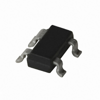
AT-32011-TR1 Avago Technologies US Inc., AT-32011-TR1 Datasheet

AT-32011-TR1
Specifications of AT-32011-TR1
Available stocks
Related parts for AT-32011-TR1
AT-32011-TR1 Summary of contents
Page 1
... BASE EMITTER SOT-23 (AT-32033) being relatively insensitive to input match. High gain capability makes these devices a good fit for 900 MHz pager applications. Voltage breakdowns are high enough for use at 5 volts. The AT-3 series bipolar transistors are fabricated using an optimized version of Agilent’ ...
Page 2
... CKT 380 CKT 380 TEST CIRCUIT BOARD MATL = 0.062" FR-4 (ε = 4.8) DIMENSIONS IN MILS Figure 1. Test Circuit for Noise Figure and Associated Gain. This circuit is a compromise match between best noise figure, best gain, stability, and a practical synthesizable match. Absolute Units Maximum V 1 ...
Page 3
... Characterization Information, T Symbol Parameters and Test Conditions P Power Gain Compression (opt tuning) 1dB Gain Gain Compression (opt tuning) 1dB Output Third Order Intercept Point (opt tuning 2 Gain in 50 Ω System 0.5 1 1.5 2 2.5 FREQUENCY (GHz) Figure 2. AT-32011 and AT-32033 Minimum Noise Figure vs ...
Page 4
... Power Gain Compression vs. Frequency and Current 2 1 100 TEMPERATURE (°C) Figure 14. AT-32011 Noise Figure and Associated Gain 2 vs. Temperature in Test C Circuit, Figure 1. (Circuit Losses De-embedded 0.5 1.0 1.5 2.0 2.5 FREQUENCY (GHz) Figure 9. AT-32011 1 dB Compressed Gain vs. Frequency and Current ...
Page 5
... AT-32011 Typical Noise Parameters, Common Emitter Ω Freq. F min GHz dB [1] 0.5 0.42 0.9 0.71 1.8 1.37 2.4 1.80 Note: 1. 0.5 GHz noise parameter values are extrapolated, not measured. AT-32033 Typical Scattering Parameters, Freq GHz Mag Ang 0.1 0.97 -11 11.09 0.5 0.81 -52 0.9 0.61 -87 1 ...
Page 6
... AT-32011 Typical Noise Parameters, Common Emitter Ω, 2 Freq. F min GHz dB [1] 0.5 0.57 0.9 0.78 1.8 1.25 2.4 1.57 Note: 1. 0.5 GHz noise parameter values are extrapolated, not measured. AT-32033 Typical Scattering Parameters, Freq GHz Mag Ang 0.1 0.93 -13 16.61 0.5 0.68 -56 14.29 0.9 ...
Page 7
... AT-32011 Typical Noise Parameters, Common Emitter Ω, 2 Freq. F min GHz dB [1] 0.5 1.39 0.9 1.51 1.8 1.78 2.4 1.96 Note: 1. 0.5 GHz noise parameter values are extrapolated, not measured. AT-32033 Typical Scattering Parameters, Freq GHz Mag Ang 0.1 0.50 -35 0.5 0.16 -52 0.9 0.08 -36 1 ...
Page 8
... AT-32011 Typical Noise Parameters, Common Emitter Ω, 2 Freq. F min GHz dB [1] 0.5 0.52 0.9 0.75 1.8 1.26 2.4 1.60 Note: 1. 0.5 GHz noise parameter values are extrapolated, not measured. AT-32033 Typical Scattering Parameters, Freq GHz Mag Ang 0.1 0.94 -13 16.56 0.5 0.69 -54 14.34 0.9 ...
Page 9
... AT-32011 Typical Noise Parameters, Common Emitter Ω Freq. F min GHz dB [1] 0.5 1.38 0.9 1.50 1.8 1.78 2.4 1.96 Note: 1. 0.5 GHz noise parameter values are extrapolated, not measured. AT-32033 Typical Scattering Parameters, Freq GHz Mag Ang 0.1 0.55 -31 0.5 0.20 -44 0.9 0.13 -31 1 ...
Page 10
... Ordering Information Part Numbers AT-32011-BLK AT-32033-BLK AT-32011-BLKG AT-32033-BLKG AT-32011-TR1 AT-32033-TR1 AT-32011-TR1G AT-32033-TR1G AT-32011-TR2 AT-32033-TR2 AT-32011-TR2G AT-32033-TR2G Note: Order part number with a “G” suffix if lead-free option is desired. Package Dimensions SOT-23 Plastic Package XXX SYMBOL A A1 Notes: XXX-package marking Drawings are not to scale No ...
Page 11
... For product information and a complete list of distributors, please go to our web site. For technical assistance call: Americas/Canada: +1 (800) 235-0312 or (916) 788-6763 Europe: +49 (0) 6441 92460 China: 10800 650 0017 Hong Kong: (65) 6756 2394 India, Australia, New Zealand: (65) 6755 1939 Japan: (+81 3) 3335-8152(Domestic/International), or ...


