SI8405DB-T1-E1 Vishay, SI8405DB-T1-E1 Datasheet
SI8405DB-T1-E1
Specifications of SI8405DB-T1-E1
Available stocks


Related parts for SI8405DB-T1-E1


SI8405DB-T1-E1 Summary of contents
Page 1
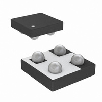
... Bump Side View Backside View Device Marking: 8405 xxx = Date/Lot Traceability Code Ordering Information: Si8405DB-T1-E1 (Lead (Pb)-free) ABSOLUTE MAXIMUM RATINGS T Parameter Drain-Source Voltage Gate-Source Voltage a Continuous Drain Current (T = 150 °C) J Pulsed Drain Current Continuous Source Current (Diode Conduction) a Maximum Power Dissipation ...
Page 2
... Si8405DB Vishay Siliconix SPECIFICATIONS °C, unless otherwise noted J Parameter Static Gate Threshold Voltage Gate-Body Leakage Zero Gate Voltage Drain Current a On-State Drain Current a Drain-Source On-State Resistance a Forward Transconductance a Diode Forward Voltage b Dynamic Total Gate Charge Gate-Source Charge Gate-Drain Charge Turn-On Delay Time ...
Page 3
... J 1 0.1 0.0 0.2 0.4 0 Source-to-Drain Voltage (V) SD Source-Drain Diode Forward Voltage Document Number: 71814 S-82118-Rev. E, 08-Sep °C J 0.8 1.0 1.2 Si8405DB Vishay Siliconix 2000 1600 C iss 1200 800 C oss C 400 rss Drain-to-Source Voltage (V) DS Capacitance 1 4 1.4 1.2 1 ...
Page 4
... Si8405DB Vishay Siliconix TYPICAL CHARACTERISTICS 25 °C, unless otherwise noted 0 250 µA D 0.3 0.2 0.1 0.0 - 0 Temperature (°C) J Threshold Voltage 2 1 Duty Cycle = 0.5 0.2 0.1 0.1 0.05 0.02 Single Pulse 0. Duty Cycle = 0.5 0.2 0.1 0.1 0.05 0.02 Single Pulse ...
Page 5
... S-82118-Rev. E, 08-Sep-08 4 0.30 0.31 Note 3 Solder Mask 0. Diamerter E a Millimeters Max. 0.650 0.290 0.360 0.410 1.600 1.600 0.850 0.380 Si8405DB Vishay Siliconix Silicon Bump Note Inches Min. Max. 0.0236 0.0256 0.0102 0.0114 0.0134 0.0142 0.0146 0.0161 0.0598 0.0630 0.0598 0.0630 0.0295 ...
Page 6
... PCB Design and Assembly Guidelines For MICRO FOOTr Products Johnson Zhao INTRODUCTION Vishay Siliconix’s MICRO FOOT product family is based on a wafer-level chip-scale packaging (WL-CSP) technology that implements a solder bump process to eliminate the need for an outer package to encase the silicon die. MICRO FOOT products include power MOSFETs, analog switches, and power ICs ...
Page 7
... BOARD LAYOUT GUIDELINES Board materials. Vishay Siliconix MICRO FOOT products are designed to be reliable on most board types, including organic boards such as FR-4 or polyamide boards. The package qualification information is based on the test on 0.5-oz. FR-4 and polyamide boards with NSMD pad design ...
Page 8
... Use a vacuum needle pick-up tip to pick up the replacement part, and use a placement jig to placed it accurately. 6. Reflow the part using the same convection nozzle, and preheat from the bottom, matching the original reflow profile. Vishay Siliconix Thermal Profile 0 100 200 300 Time (Seconds FIGURE 6 ...
Page 9
... Vishay product could result in personal injury or death. Customers using or selling Vishay products not expressly indicated for use in such applications their own risk and agree to fully indemnify and hold Vishay and its distributors harmless from and against any and all claims, liabilities, expenses and damages arising or resulting in connection with such use or sale, including attorneys fees, even if such claim alleges that Vishay or its distributor was negligent regarding the design or manufacture of the part ...