ADNS-3530 Avago Technologies US Inc., ADNS-3530 Datasheet
ADNS-3530
Specifications of ADNS-3530


Related parts for ADNS-3530


ADNS-3530 Summary of contents
Page 1
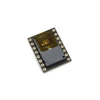
... ADNS-3530 Low Power LED Integrated Slim Mouse Sensor Data Sheet Description The ADNS-3530 LED optical mouse sensor is a small form factor (SFF) LED illuminated navigation system. The ADNS-3530 is a low-power optical navigation sen- sor. It has a new, low-power architecture and automatic power management modes, making it ideal for battery- and power-sensitive applications such as cordless input devices ...
Page 2
... Pinout of ADNS-3530 Optical Mouse Sensor Pin Name Description 1 MISO Serial Data Output (Master In/Slave Out) 2 SCLK Serial Clock Input 3 MOSI Serial Data Input (Master Out/Slave In) 4 MOTION Motion Detect (Active Low Output) 5 XY_LED LED Control 6 LED_GND Ground for LED Current 7 SHTDWN ...
Page 3
C L (0.38) 0.80 (0.03) 0.50 (0.020) 1.19 (0.047) OPTICAL CENTER C L GUIDE HOLE A 1.95 (0.08) 1.70 (0.07) Figure 2. Package outline drawing CAUTION advised that normal static precautions be taken in handling ...
Page 4
... PCB alignment. The components interlock as they are mounted onto defined features on the base plate. The ADNS-3530 sensor is designed for surface mounting on a PCB, looking down. There is an aperture stop and features on the package that align to the lens. The ADNS-3150-001 lens provides optics for the imag- ing of the surface as well as illumination of the surface at the optimum angle ...
Page 5
... Figure 5a. Exploded top view Figure 5b. Exploded bottom view 5 ADNS-3530 ADNS-3150-001 CUSTOMER- SUPPLIED BASE PLATE ADNS-3530 ADNS-3150-001 CUSTOMER- SUPPLIED BASE PLATE ...
Page 6
... Design Considerations for Improved ESD Performance For improved electrostatic discharge performance, typi- cal creepage and clearance distance are shown in the table below. Assumption: base plate construction as per the Avago Technologies supplied IGES file and ADNS- 3150-001 lens. Typical Distance Creepage Clearance ...
Page 7
7 ...
Page 8
Regulatory Requirements • Passes FCC B and worldwide analogous emission limits when assembled into a mouse with shielded cable and following Avago Technologies recommendations. • Passes IEC-1000-4-3 radiated susceptibility level when assembled into a mouse with shielded cable and fol- ...
Page 9
AC Electrical Specifications Electrical Characteristics over recommended operating conditions. Typical values at 25°C, V Parameter Symbol Motion Delay After Reset t MOT-RST Shutdown t SHTDWN Wake from Shutdown t WAKEUP Forced Rest Enable t REST-EN Wake from Forced Rest t ...
Page 10
... I leak Current Output Low Voltage V OL Output High Voltage V OH Input Capacitance C in ADNS-3530 RESOLUTION 700 600 500 400 300 200 100 0 0.77 0.87 0.97 1.07 1.17 1.27 1.37 1.47 1.57 1.67 1.77 1.87 1.97 Z-HEIGHT (mm) Figure 9. Mean resolution vs. Z TYPICAL PATH DEVIATION LARGEST SINGLE PERPENDICULAR DEVIATION FROM A STRAIGHT LINE AT 45 DEGREES PATH LENGTH = 4 INCHES ...
Page 11
... ADNS-3530 will flash the LED only when needed. Synchronous Serial Port The synchronous serial port is used to set and read pa- rameters in the ADNS-3530, and to read out the motion information. The port is a four wire serial port. The host microcon- troller always initiates communication; the ADNS-3530 never initiates data transfers ...
Page 12
... MOSI, and has a “0” as its MSB to indicate data direction. The second byte contains the data and is driven by the ADNS-3530 over MISO. The sensor outputs MISO bits on falling edges of SCLK and samples MOSI bits on every rising edge of SCLK. ...
Page 13
... MISO data hold time of the ADNS-3530. Since the falling edge of SCLK is actually the start of the next read or write command, the ADNS-3530 will hold the state of data on MISO until the falling edge of SCLK. Required Timing Between Read and Write Commands There are minimum timing requirements between read and write commands on the serial port ...
Page 14
... SRAD ADNS-3530 has time to prepare the requested data. The falling edge of SCLK for the first address bit of either the read or write command must be at least t ter the last SCLK rising edge of the last data bit of the previous read operation ...
Page 15
... Configuration_Bits register (0x11). This is to allow for further power savings in applications where the sensor does not need to operate all the time. The ADNS-3530 can be set in Shutdown mode by as- serting the SHTDWN pin. For proper operation, SHTD- WN pulse width must be at least t SHTDWN widths may cause the chip to enter an undefined state ...
Page 16
... Registers The ADNS-3530 registers are accessible via the serial port. The registers are used to read motion data and status as well as to set the device configuration. Address Register 0x00 Product_ID 0x01 Revision_ID 0x02 Motion 0x03 Delta_Y 0x04 Delta_X 0x05 SQUAL 0x06 Shutter_Upper ...
Page 17
Revision_ID Address: 0x01 Access: Read Reset Value: 0x02 Bit 7 Field RID 7 Data Type: 8-bit unsigned integer USAGE: This register contains the IC revision subject to change when new IC versions are released. Motion Address: 0x02 Access: ...
Page 18
Delta_Y Address: 0x03 Access: Read Reset Value: Undefined Bit 7 6 Field Data Type: Eight bit 2’s complement number USAGE: Y movement is counts since last report. Absolute value is determined by resolution. Reading clears the ...
Page 19
SQUAL Address: 0x05 Access: Read Reset Value: Undefined Bit 7 6 Field Data Type: Upper 8 bits of a 9-bit unsigned integer USAGE: SQUAL (Surface Quality measure of the number of valid features visible ...
Page 20
Pixel_Sum Address: 0x09 Access: Read Reset Value: Undefined Bit 7 6 Field Data Type: High 8 bits of an unsigned 17-bit integer USAGE: This register is used to find the average pixel value. It reports the ...
Page 21
... Array Map Looking Through the ADNS-3150-001 Lens) 462 461 439 417 395 373 351 329 307 285 263 241 463 460 438 416 394 372 350 328 306 284 262 240 464 459 437 415 393 371 349 327 305 ...
Page 22
CRC2 Address: 0x0e Access: Read Reset Value: Undefined Bit 7 6 Field CRC2 CRC2 7 Data Type: Eight-bit number USAGE: Register 0x0e reports the third byte of the system self test results. Value = 0x31. See Self Test register 0x10. ...
Page 23
Configuration_bits Address: 0x11 Access: Read/Write Reset Value: 0x03 Bit 7 Field RES Reserved Data Type: Bit field USAGE: Register 0x11 allows the user to change the configuration of the sensor. Setting the RESTEN bit forces the sensor into Rest mode, ...
Page 24
Observation Address: 0x2e Access: Read/Write Reset Value: Undefined Bit 7 Field MODE MODE 1 Data Type: Bit field USAGE: Register 0x2e provides bits that are set every frame. It can be used during EFTB testing to check that the chip ...
Page 25
Inverse_Revision_ID Address: 0x3e Access: Read Reset Value: 0xFD Bit 7 Field NRID NRID 7 Data Type: nverse 8-bit unsigned integer USAGE: This value is the inverse of the Revision_ID. It can be used to test the SPI port. Inverse_Revision_ID Address: ...