ADNS-5050 Avago Technologies US Inc., ADNS-5050 Datasheet - Page 12
ADNS-5050
Manufacturer Part Number
ADNS-5050
Description
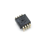
8 DIP SFF Navigation Sensor
Manufacturer
Avago Technologies US Inc.
Datasheet
1.ADNK-5050.pdf
(26 pages)
Specifications of ADNS-5050
Lead Free Status / RoHS Status
Lead free / RoHS Compliant
Lead Free Status / RoHS Status
Lead free / RoHS Compliant
Other names
516-2261
ADNS-5050
ADNS-5050
Available stocks
Company
Part Number
Manufacturer
Quantity
Price
Company:

Part Number:
ADNS-5050
Manufacturer:
RELALTEK
Quantity:
414
Part Number:
ADNS-5050
Manufacturer:
原装AVAGO
Quantity:
20 000


LED Mode
For optimized tracking performance, the LED is in DC
mode when motion is detected, and ADNS-5050 will pulse
the LED when the mouse is in idle state. To force the LED
into always DC mode, kindly refer to register 0x22.
Synchronous Serial Port
The synchronous serial port is used to set and read pa-
rameters in the ADNS-5050, and to read out the motion
information.
The port is a three wire serial port. The host micro-con-
troller always initiates communication; the ADNS-5050
never initiates data transfers. SCLK, SDIO, and NCS may be
driven directly by a micro-controller. The port pins may be
shared with other SPI slave devices. When the NCS pin is
high, the inputs are ignored and the output is tri-stated.
The lines that comprise the SPI port:
SCLK:
SDIO:
NCS:
Write Operation
SDIO Setup and Hold Time
12
SCLK
SDIO
NCS
SCLK
SDIO
1/(2f
Clock input. It is always generated by the master
(the micro-controller).
Input and Output data.
Chip select input (active low). NCS needs to be low
to activate the serial port; otherwise, SDIO will be
high Z, and SDIO & SCLK will be ignored. NCS can
also be used to reset the serial port in case of an
error.
t
SCLK
setup
)
1
1
1/(2f
t
hold
A 6
SCLK
2
)
3
A 5
A 4
4
A 3
5
SDIO DRIVEN BY MICRO-CONTROLLER
A 2
6
A 1
7
A 0
8
D 7
9
10
D 6
Chip Select Operation
The serial port is activated after NCS goes low. If NCS
is raised during a transaction, the entire transaction is
aborted and the serial port will be reset. This is true for
all transactions. After a transaction is aborted, the normal
address-to-data or transaction-to-transaction delay is still
required before beginning the next transaction. To improve
communication reliability, all serial transactions should be
framed by NCS. In other words, the port should not remain
enabled during periods of non-use because ESD and EFT/B
events could be interpreted as serial communication and
put the chip into an unknown state. In addition, NCS must
be raised after each burst-mode transaction is complete to
terminate burst-mode. The port is not available for further
use until burst-mode is terminated.
Write Operation
Write operation, defined as data going from the micro-
controller to the ADNS-5050, is always initiated by the
micro-controller and consists of two bytes. The first byte
contains the address (seven bits) and has a “1” as its MSB to
indicate data direction. The second byte contains the data.
The ADNS-5050 reads SDIO on rising edges of SCLK.
11
D 5
12
D 4
13
D 3
14
D 2
15
D 1
16
D 0
1
1
A 6
2
Related parts for ADNS-5050
Image
Part Number
Description
Manufacturer
Datasheet
Request
R

Part Number:
Description:
Optical Mouse Sensor,DIP
Manufacturer:
Avago Technologies US Inc.
Datasheet:

Part Number:
Description:
Optical Mouse Sensor,DIP
Manufacturer:
Avago Technologies US Inc.
Datasheet:

Part Number:
Description:
Low Power Wireless LED Sensor
Manufacturer:
Avago Technologies US Inc.
Datasheet:
Part Number:
Description:
USB SoC 3B Optical Sensor
Manufacturer:
Avago Technologies US Inc.
Datasheet:
Part Number:
Description:
Low Power Wireless LED Sensor
Manufacturer:
Avago Technologies US Inc.
Datasheet:
Part Number:
Description:
Optical Mouse Sensor,DIP
Manufacturer:
Avago Technologies US Inc.
Datasheet:

Part Number:
Description:
Trim Lens For ADNS-3530
Manufacturer:
Avago Technologies US Inc.
Datasheet:

Part Number:
Description:
Trim Lens For ADNS-5090
Manufacturer:
Avago Technologies US Inc.
Datasheet:

Part Number:
Description:
BLACK CLIP FOR ADNS-5000
Manufacturer:
Avago Technologies US Inc.
Datasheet:
Part Number:
Description:
Lens For ADNS-7630
Manufacturer:
Avago Technologies US Inc.
Datasheet:

Part Number:
Description:
OPTOCOUPLER GATE DRV 2A 16-SOIC
Manufacturer:
Avago Technologies US Inc.
Datasheet:
Part Number:
Description:
OPTOCOUPLER 2CH 2.5A 16-SOIC
Manufacturer:
Avago Technologies US Inc.
Datasheet:

Part Number:
Description:
OPTOCOUPLER GATE DRV 0.4A 16SOIC
Manufacturer:
Avago Technologies US Inc.
Datasheet:

Part Number:
Description:
OPTOCOUPLER 2.0A 250KHZ 8-DIP
Manufacturer:
Avago Technologies US Inc.
Datasheet:

Part Number:
Description:
OPTOCOUPLER 2.0A 250KHZ GW 8-SMD
Manufacturer:
Avago Technologies US Inc.
Datasheet: