ADNS-7550 Avago Technologies US Inc., ADNS-7550 Datasheet
ADNS-7550
Specifications of ADNS-7550
ADNS-7550
Available stocks


Related parts for ADNS-7550


ADNS-7550 Summary of contents
Page 1
... ADNS-7550 Integrated molded lead-frame DIP Sensor Data Sheet Theory of Operation The ADNS-7550 integrated molded lead-frame DIP sensor comprises of sensor and VCSEL in a single package. The advanced class of VCSEL was engineered by Avago Technologies to provide a laser diode with a single lon- gitudinal and a single transverse mode. In contrast to ...
Page 2
... IO Voltage input (1.65~3.6V) 16 VCSEL-VE Negative Terminal of VCSEL 2 VCSEL +VE 1 LASER_NEN 2 A7550 NCS 3 MISO 4 SCLK 5 MOSI 6 MOTION 7 XYYWWZV XYLASER Subcon Code YYWW = Date Code Z = Sensor Die Source V = VCSEL Die Source KL = VCSEL Binning Figure 1. Device pin-out for ADNS-7550 16 VCSEL -VE VDDIO 15 DGND 14 RefA 13 RefB 12 GND VDD5 9 ...
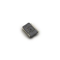
Page 3
Figure 2. Package outline drawing CAUTION advised that normal static precautions be taken in handling and assembly of this component to prevent damage and/or degradation which may be induced by ESD 3 ...
Page 4
... LASER Drive XYLASER VCSEL-VE VCSEL Figure 3. Block diagram of ADNS-7550 integrated molded lead-frame DIP sensor Figure 4. 2D Assembly drawing of ADNS-7550 sensor coupled with the ADNS-6150 lens, PCB and base plate (top and cross-sectional view) 4 Regulatory Requirements x Passes FCC B and worldwide analogous emission limits ...
Page 5
... Design considerations for improving ESD Performance For improved electrostatic discharge performance, typical creepage and clearance distance are shown in the table below. Assumption: base plate construction as per the Avago supplied IGES file and ADNS-6150, ADNS- 6160-001 or ADNS-6170-002 lens: Lens ADNS-6150 Creepage 12 ...
Page 6
VDDIO 15 B REF DGND 12 14 VDD5 GND VCC 1 SPCP868A GND ...
Page 7
... The laser is driven in pulsed mode during normal operation. A calibration mode is provided which drives the laser in continuous (CW) operation. Eye Safety The ADNS-7550 integrated molded lead-frame DIP sensor and the associated components in the schematic of Figure 5 are intended to comply with Class 1 Eye Safety Requirements of IEC 60825-1. Avago Technologies suggests that manufacturers perform testing to verify eye safety on each mouse ...
Page 8
... RefB at XYLASER), LASER_NEN goes high to turn the transistor off and dis- connect RefB from the LASER. Single Fault Detection ADNS-7550 is able to detect a short circuit or fault condition at the XYLASER pin, which could lead to excessive laser power output. A path to ground on this Microcontroller ...
Page 9
Absolute Maximum Ratings Parameter Symbol Storage Temperature T S Lead Soldering Temperature T Solder Supply Voltage V DD3 V DDIO ESD (Human-body model) V ESD Input Voltage V IN Latchup Current I OUT VCSEL Die Source Marking Parameter (For VCSEL ...
Page 10
Optical/Electrical Characteristics ( 5°C to 45°C): VCSEL Die Source Marking V = A,V Parameter Symbol Min Peak Wavelength λ 832 Maximum Radiant LOPmax Power Wavelength dλ/dT Temperature coef- ficient Wavelength dλ/dI Current coefficient Beam Divergence θFW@1/ e^2 Threshold ...
Page 11
Figure 9. Recommended Soldering Reflow Profile DC Electrical Specifications Electrical Characteristics over recommended operating conditions. (Typical values at 25 °C, V Parameter Symbol DC Supply Current I DD_RUN in various modes Peak Supply Current Shutdown Supply I DDSTDWN Current Input ...
Page 12
AC Electrical Specifications Electrical Characteristics over recommended operating conditions. (Typical values at 25 °C, VDD=5.0V, VDDIO= 2.8V) Parameter Symbol Minimum Typical Motion delay t MOT-RST after reset Shutdown t STDWN Wake from t 23 WAKEUP shutdown MISO rise time t ...
Page 13
Resolution vs Z- Height on General Surfaces (A7550) 1200 1000 800 600 400 200 0 -0.3 -0.2 Figure 10. Mean Resolution vs 800cpi Typical Path Deviation Largest Single Perpendicular Deviation From A Straight Line at 45 Degrees Path ...
Page 14
... Synchronous Serial Port (mA) F The synchronous serial port is used to set and read pa- rameters in the ADNS-7550, and to read out the motion information. The port is a four-wire port. micro-controller always initiates communication; the ADNS-7550 never initiates data transfers. SCLK, MOSI, and NCS may be driven directly by a micro-controller. ...
Page 15
... The 0.5/fSCLK minimums high state of SCLK is also the minimum MISO data hold time of the ADNS-7550. Since the falling edge of SCLK is actually the start of the next read or write command, the ADNS-7550 will hold the state of data on MISO until the falling edge of SCLK. 15 ...
Page 16
... The speed improvement is achieved by continuous data clocking to or from multiple registers without the need to specify the register address, and by not requiring the normal delay period between data bytes. Burst mode is activated by reading the Motion_Burst register. The ADNS-7550 will respond with the contents of the Motion, Delta_X_L, Delta_Y_L, Delta_XY_H, SQUAL, Shutter_Upper, Shutter_Lower and Maximum_Pixel registers in that order ...
Page 17
... NEN Undefined Undefined Undefined Functional 17 Notes on Shutdown The ADNS-7550 can be set in Shutdown mode by writing 0xe7 to register 0x3b. The SPI port should not be accessed when Shutdown mode is asserted, except the power-up command (writing 0x5a to register 0x3a). (Other ICs on the same SPI bus can be accessed, as long as the sensor’ ...
Page 18
... Registers The ADNS-7550 registers are accessible via the serial port. The registers are used to read motion data and status as well as to set the device configuration. Address Register 0x00 Product_ID 0x01 Revision_ID 0x02 Motion 0x03 Delta_X_L 0x04 Delta_Y_L 0x05 Delta_XY_H 0x06 SQUAL ...
Page 19
... Field PID PID 7 6 Data Type: 8-Bit unsigned integer USAGE: This register contains a unique identification assigned to the ADNS-7550. The value in this register does not change; it can be used to verify that the serial communications link is functional. Revision_ID Access: Read Bit 7 6 Field ...
Page 20
Motion Access: Read/Write Bit 7 6 Field MOT PIXRDY Data Type: Bit field. USAGE: Register 0x02 allows the user to determine if motion has occurred since the last time it was read. If the MOT bit is set, then the ...
Page 21
Delta_X_L Access: Read Bit 7 6 Field Data Type: Eight bit 2’s complement number. USAGE: X movement is counts since last report. Absolute value is determined by resolution. Reading clears the register. -2048 -2047 Motion 800 ...
Page 22
SQUAL Access: Read Bit 7 6 Field Data Type: Upper 8 bits of a 9-bit unsigned integer. USAGE: SQUAL (Surface Quality measure of the number of valid features visible by the sensor in the ...
Page 23
Shutter_Upper Access: Read Bit 7 6 Field Shutter_Lower Access: Read Bit 7 6 Field Data Type: Sixteen bit unsigned integer. USAGE: Units are clock cycles. Read Shutter_Upper first, then Shutter_Lower. They should ...
Page 24
Maximum_Pixel Access: Read Bit 7 6 Field Data Type: Eight-bit number. USAGE: Maximum Pixel value in current frame. Minimum value = 0, maximum value = 254. The maximum pixel value can vary with every frame. Pixel_Sum ...
Page 25
CRC0 Address: 0x0c Access: Read Reset Value: 0x00 Bit 7 6 Field CRC0 CRC0 7 6 Data Type: Eight-bit number. USAGE: Register 0x0c reports the first byte of the system self test results. Value = F4. CRC1 Address: 0x0d Access: ...
Page 26
Self_Test Address: 0x10 Access: Write Reset Value: NA Bit 7 6 Field Reserved Reserved Data Type: Bit field USAGE: Before performing system self test, reset the chip. Then, set the TESTEN bit in register 0x10 to start the system self ...
Page 27
LASER_CTRL0 Access: Read/Write Bit 7 6 Field Range1 Range0 Data Type: Bit field USAGE: This register is used to control the laser drive. Bits 7 and 6 require complement values in register 0x1F. If the registers do not contain complementary ...
Page 28
LSRPWR_CFG0 Address: 0x1c Access: Read/Write Reset Value: 0x00 Bit 7 6 Field Data Type: 8 Bit unsigned USAGE: This register is used to set the laser current used together with register 0x1D, ...
Page 29
LASER_CTRL1 Address: 0x1f Access: Read/Write Reset Value: 0x00 Bit 7 6 Field Range_C1 Range_C0 Data Type: 8 Bit unsigned USAGE: Bits 7 and 6 of this register must be the complement of the corresponding bits in register 0x1A for the ...
Page 30
Pixel_Grab Address: 0x35 Access: Read/Write Reset Value: 0x00 Bit 7 6 Field Data Type: 8 Bit Word USAGE: For test purposes, the sensor will read out the contents of the pixel array, one pixel per frame. ...
Page 31
H_RESOLUTION Address: 0x36 Access: Read/Write Reset Value: 0x04 Bit 7 6 Field Reserved Reserved Data Type : Bit field USAGE : This register is used to set the resolution configuration of sensor up to 2000cpi. For resolution setting at 1600cpi ...
Page 32
Shut_thr Access: Read/Write Bit 7 6 Field Shut_thr Shut_thr 7 Data Type: 7 Bit number USAGE: Threshold defines the Shutter value when lifted runaway happens. Sensor will suspect lifted runaway happens and suppress motion if (Shutter > Shut_thr[7:1]*32). Inverse_Revision_ID Access: ...